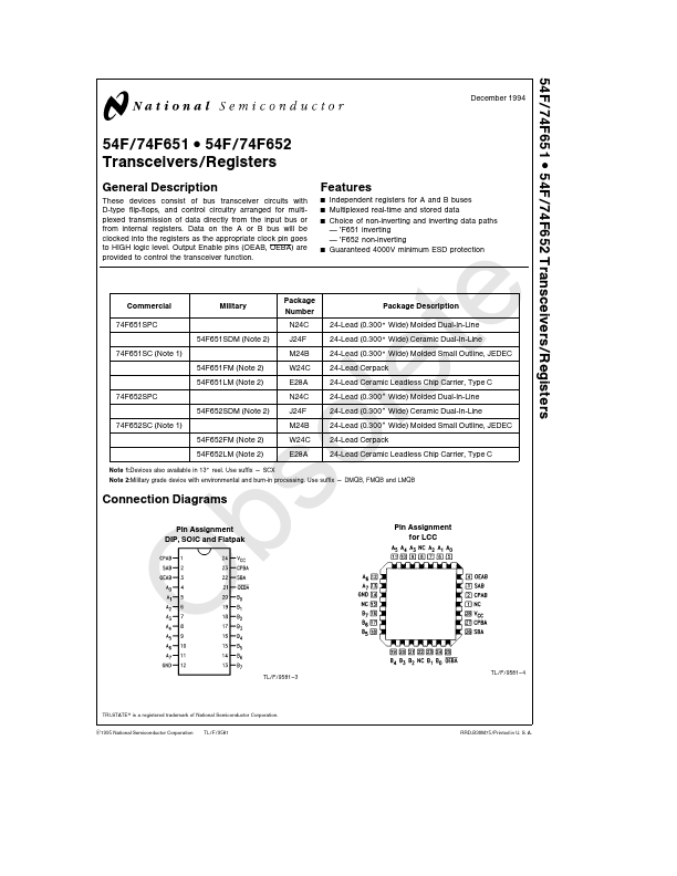
54F651 Key Features
- 4 RRD-B30M75 Printed in U S A
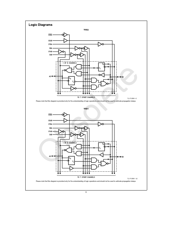
- 5 Please note that this diagram is provided only for the understanding of logic operations and should not be used to est
- 12 Please note that this diagram is provided only for the understanding of logic operations and should not be used to es