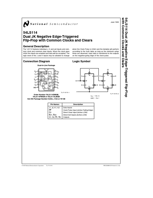
Datasheet4U Logo Datasheet4U.com

54LS114 - Dual JK Flip-Flop

Description

The ’LS114

Features

  • individual J K and set inputs and common clock and common clear inputs When the clock goes HIGH the inputs are enabled and data will be accepted The logic level of the J and K inputs may be allowed to change when the Clock Pulse is HIGH and the bistable will perform according to the truth table as long as the minimum setup times are observed Input data is transferred to the outputs on the negative-going edge of the clock pulse Connection Diagram Dual-In-Line Package Logic Symbol TL F 10176.

📥 Download Datasheet

Datasheet preview – 54LS114
Other Datasheets by National Semiconductor

Full PDF Text Transcription

Click to expand full text
54LS114 Dual JK Negative Edge-Triggered Flip-Flop with Common Clocks and Clears June 1989 54LS114 Dual JK Negative Edge-Triggered Flip-Flop with Common Clocks and Clears General Description The ’LS114 features individual J K and set inputs and common clock and common clear inputs When the clock goes HIGH the inputs are enabled and data will be accepted The logic level of the J and K inputs may be allowed to change when the Clock Pulse is HIGH and the bistable will perform according to the truth table as long as the minimum setup times are observed Input data is transferred to the outputs on the negative-going edge of the clock pulse Connection Diagram Dual-In-Line Package Logic Symbol TL F 10176 – 1 Order Number 54LS114DMQB 54LS114FMQB or 54LS114LMQB See NS Package Number E20A J14A
Published: |