7493 Overview
Key Specifications
Max Operating Temp: 150 °C
Min Operating Temp: -65 °C
Description
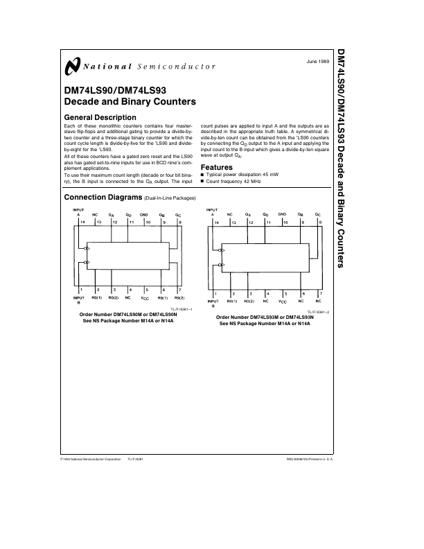
Each of these monolithic counters contains four masterslave flip-flops and additional gating to provide a divide-bytwo counter and a three-stage binary counter for which the count cycle length is divide-by-five for the ’LS90 and divideby-eight for the ’LS93 All of these counters have a gated zero reset and the LS90 also has gated set-to-nine inputs for use in BCD nine’s complement applications To use their maximum count length (decade or four bit binary) the B input is connected to the QA output The input count pulses are applied to input A and the outputs are as described in the appropriate truth table A symmetrical divide-by-ten count can be obtained from the ’LS90 counters by connecting the QD output to the A input and applying the input count to the B input which gives a divide-by-ten square wave at output QA.