March 1993
74ACQ377 54ACTQ 74ACTQ377
Quiet Series Octal D Flip-Flop with Clock Enable
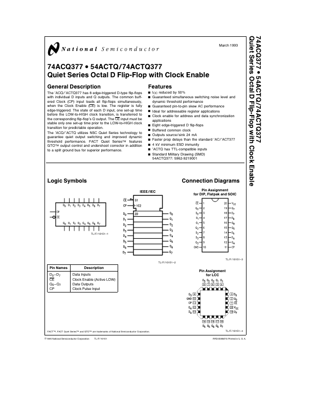
General Description
The ’ACQ ’ACTQ377 has 8 edge-triggered D-type flip-flops
with individual D inputs and Q outputs The common buff-
ered Clock (CP) input loads all flip-flops simultaneously
when the Clock Enable (CE) is low The register is fully
edge-triggered The state of each D input one set-up time
before the LOW-to-HIGH clock transition is transferred to
the corresponding flip-flop’s Q output The CE input must be
stable only one set-up time prior to the LOW-to-HIGH clock
transition for predictable operation
The ’ACQ ’ACTQ utilizes NSC Quiet Series technology to
guarantee quiet output switching and improved dynamic
threshold performance FACT Quiet SeriesTM features
GTOTM output control and undershoot corrector in addition
to a split ground bus for superior performance
Features
Y ICC reduced by 50%
Y Guaranteed simultaneous switching noise level and
dynamic threshold performance
Y Guaranteed pin-to-pin skew AC performance
Y Ideal for addressable register applications
Y Clock enable for address and data synchronization
applications
Y Eight edge-triggered D flip-flops
Y Buffered common clock
Y Outputs source sink 24 mA
Y Faster prop delays than the standard ’AC ’ACT377
Y 4 kV minimum ESD immunity
Y ’ACTQ has TTL-compatible inputs
Y Standard Military Drawing (SMD)
54ACTQ377 5962-9219001
Logic Symbols
IEEE IEC
Connection Diagrams
Pin Assignment
for DIP Flatpak and SOIC
TL F 10151 – 1
Pin Names
D0 – D7
CE
Q0 – Q7
CP
Description
Data Inputs
Clock Enable (Active LOW)
Data Outputs
Clock Pulse Input
TL F 10151 – 2
TL F 10151 – 3
Pin Assignment
for LCC
FACTTM FACT Quiet SeriesTM and GTOTM are trademarks of National Semiconductor Corporation
C1995 National Semiconductor Corporation TL F 10151
TL F 10151 – 4
RRD-B30M75 Printed in U S A