74ACTQ08
Description
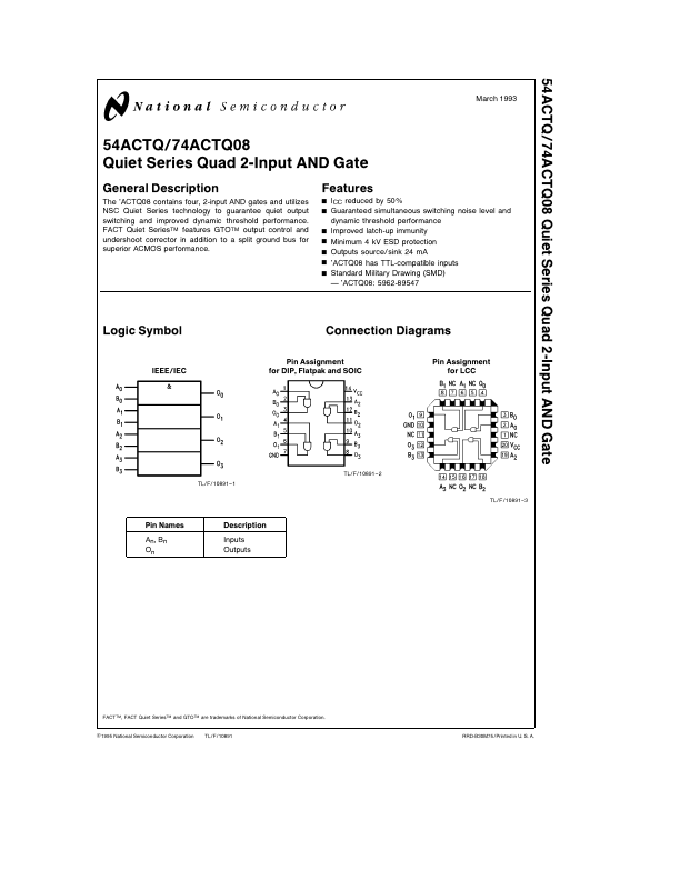
The ’ACTQ08 contains four 2-input AND gates and utilizes NSC Quiet Series technology to guarantee quiet output switching and improved dynamic threshold performance FACT Quiet SeriesTM features GTOTM output control and undershoot corrector in addition to a split ground bus for superior ACMOS performance.