74F192 Overview
Key Specifications
Package: SOP
Operating Voltage: 5 V
Max Voltage (typical range): 5.5 V
Min Voltage (typical range): 4.5 V
Description
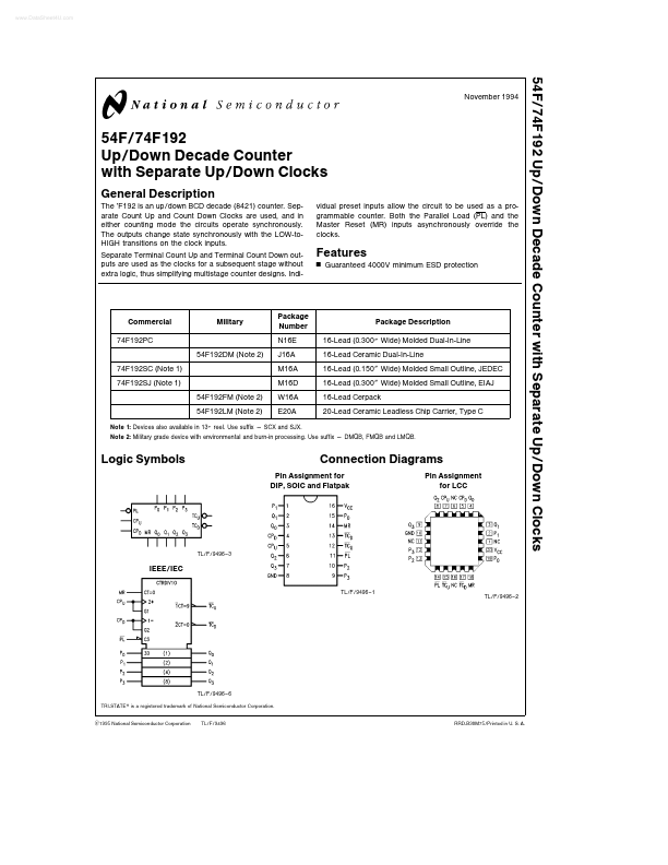
The ’F192 is an up down BCD decade (8421) counter Separate Count Up and Count Down Clocks are used and in either counting mode the circuits operate synchronously The outputs change state synchronously with the LOW-toHIGH transitions on the clock inputs Separate Terminal Count Up and Terminal Count Down outputs are used as the clocks for a subsequent stage without extra logic thus simplifying multistage counter designs Individual preset inputs allow the circuit to be used as a programmable counter Both the Parallel Load (PL) and the Master Reset (MR) inputs asynchronously override the clocks.
Key Features
- 74F192SC (Note
- 74F192SJ (Note
- 54F192FM (Note
- 54F192LM (Note