Datasheet4U Logo Datasheet4U.com

CD4007M - Dual Complementary Pair Plus Inverter

Description

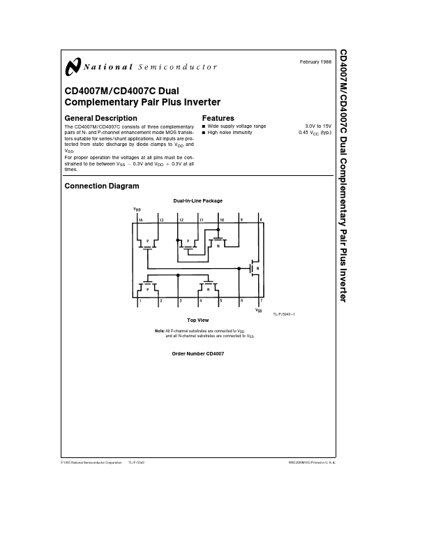
The CD4007M CD4007C consists of three complementary pairs of N- and P-channel enhancement mode MOS transistors suitable for series shunt applications All inputs are protected from static discharge by diode clamps to VDD and VSS For proper operation the voltages at all pins must be constrained to be

Features

  • Y Y Wide supply voltage range High noise immunity 3 0V to 15V 0 45 VCC (typ ) Connection Diagram Dual-In-Line Package TL F 5943.
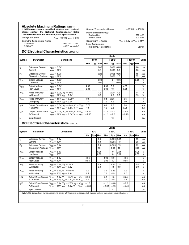
  • 1 Top View Note All P-channel substrates are connected to VDD and all N-channel substrates are connected to VSS Order Number CD4007 C1995 National Semiconductor Corporation TL F 5943 RRD-B30M105 Printed in U S A Absolute Maximum Ratings (Note 1) If Military Aerospace specified devices are required please contact the National Semiconductor Sales Offic.

📥 Download Datasheet

Other Datasheets by National Semiconductor

Full PDF Text Transcription

Click to expand full text
CD4007M CD4007C Dual Complementary Pair Plus Inverter February 1988 CD4007M CD4007C Dual Complementary Pair Plus Inverter General Description The CD4007M CD4007C consists of three complementary pairs of N- and P-channel enhancement mode MOS transistors suitable for series shunt applications All inputs are protected from static discharge by diode clamps to VDD and VSS For proper operation the voltages at all pins must be constrained to be between VSS b 0 3V and VDD a 0 3V at all times Features Y Y Wide supply voltage range High noise immunity 3 0V to 15V 0 45 VCC (typ ) Connection Diagram Dual-In-Line Package TL F 5943 – 1 Top View Note All P-channel substrates are connected to VDD and all N-channel substrates are connected to VSS Order Number CD4007 C1995 National Semiconductor C
Published: |