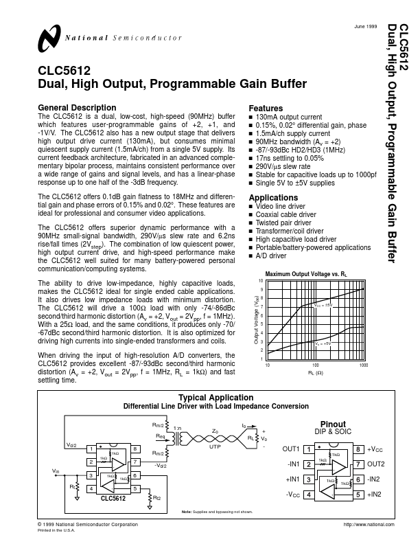
CLC5612 Overview
The CLC5612 is a dual, low-cost, high-speed (90MHz) buffer which.
CLC5612 datasheet by National Semiconductor (now Texas Instruments).
| Part number | CLC5612 |
|---|---|
| Datasheet | CLC5612_NationalSemiconductor.pdf |
| File Size | 208.22 KB |
| Manufacturer | National Semiconductor (now Texas Instruments) |
| Description | Dual/ High Output/ Programmable Gain Buffer |
|
|
The CLC5612 is a dual, low-cost, high-speed (90MHz) buffer which.
View all National Semiconductor (now Texas Instruments) datasheets
| Part Number | Description |
|---|---|
| CLC5602 | Dual/ High Output/ Video Amplifier |
| CLC5622 | Dual/ High Output/ Video Amplifier |
| CLC5623 | Video Amplifier |
| CLC5632 | Programmable Gain Buffer |
| CLC5633 | Triple/ High Output/ Programmable Gain Buffer |
| CLC5644 | Low-Power/ Low-Cost/ Quad Operational Amplifier |
| CLC5654 | Very High-Speed/ Low-Cost/ Quad Operational Amplifier |
| CLC5665 | Low Distortion Amplifier with Disable |
| CLC501 | High-Speed Output Clamping Op Amp |
| CLC502 | Clamping/ Low-Gain Op Amp with Fast 14-bit Settling |