Datasheet Summary
54LS174 DM54LS174 DM74LS174 54LS175 DM54LS175 DM74LS175 Hex Quad D Flip-Flops with Clear
June 1989
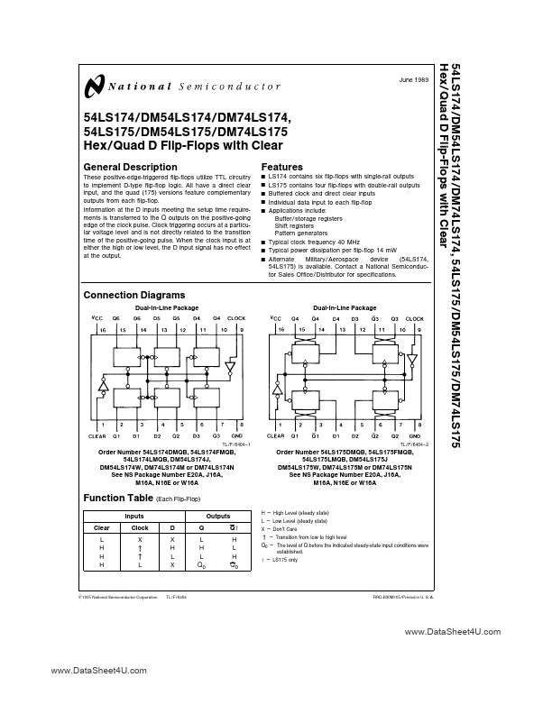
54LS174 DM54LS174 DM74LS174 54LS175 DM54LS175 DM74LS175 Hex Quad D Flip-Flops with Clear
General Description
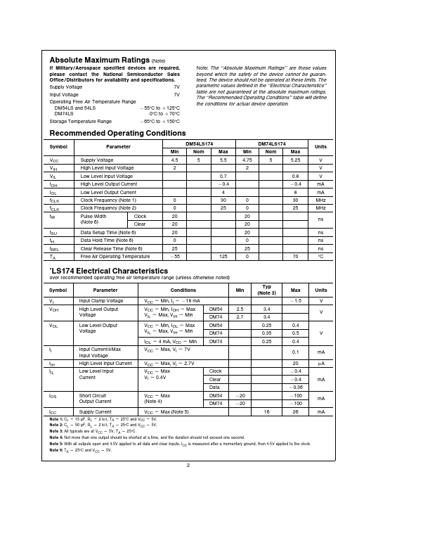
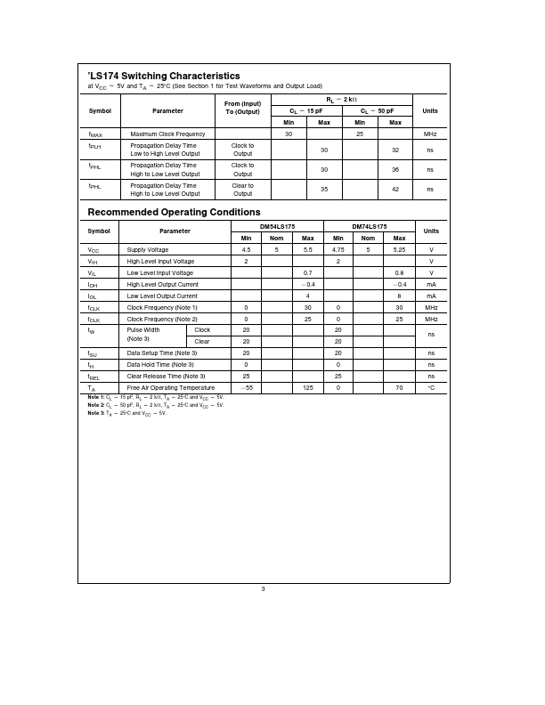
These positive-edge-triggered flip-flops utilize TTL circuitry to implement D-type flip-flop logic All have a direct clear input and the quad (175) versions feature plementary outputs from each flip-flop Information at the D inputs meeting the setup time requirements is transferred to the Q outputs on the positive-going edge of the clock pulse Clock triggering occurs at a particular voltage level and is not directly related to the transition time of the positive-going pulse When...