NJM3776D2 Overview
Key Specifications
Description
GND 1 "Power Ground" from output channel 1. Connected to the ground path (see application examples).
Key Features
- Suitable to drive any external MOS FET or bipolar power transistor
- Cross conduction prevented by time delay
- Digital filter on chip eliminates external filtering components
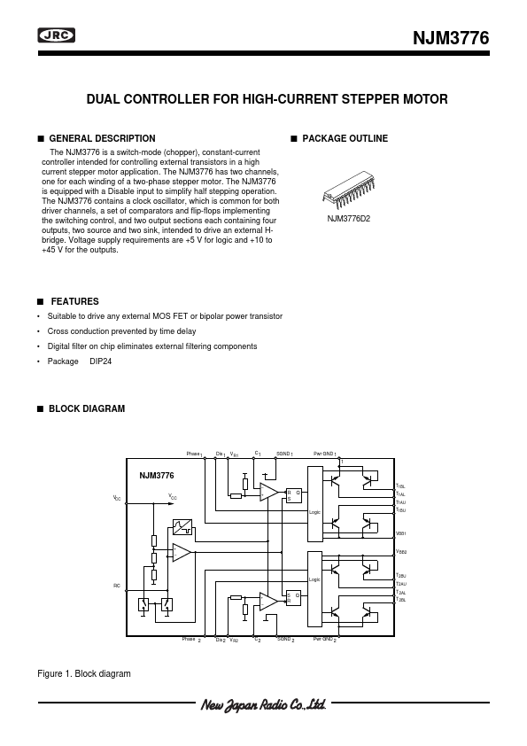
- Package DIP24 s Phase 1 Dis 1 VR1 C1 SGND 1 Pwr GND 1 1 NJM3776 VCC V CC – + RQ S Logic RC Figure