P55N02LD Overview
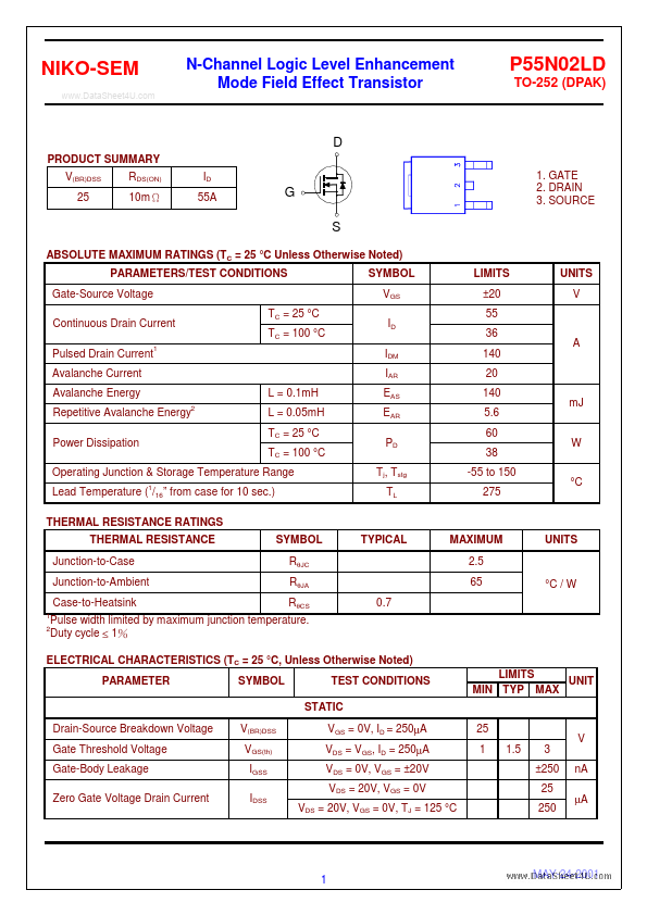
N-Channel Logic Level Enhancement Mode Field Effect Transistor P55N02LD TO-252 (DPAK) D PRODUCT SUMMARY V(BR)DSS 25 RDS(ON) 10mΩ ID 55A 1. Pulse Width ≤ 300 µsec, Duty Cycle ≤ 2%. Independent of operating temperature.
| Part number | P55N02LD |
|---|---|
| Datasheet | P55N02LD_Niko.pdf |
| File Size | 77.65 KB |
| Manufacturer | Niko |
| Description | N-Channel Logic Level Enhancement |
|
|
N-Channel Logic Level Enhancement Mode Field Effect Transistor P55N02LD TO-252 (DPAK) D PRODUCT SUMMARY V(BR)DSS 25 RDS(ON) 10mΩ ID 55A 1. Pulse Width ≤ 300 µsec, Duty Cycle ≤ 2%. Independent of operating temperature.