MSM5424331 Description
The MSM5424331 is an image data processing field memory organized as 222,720 (768 pixels by 290 lines) by 24 bits that can switch between the FIFO mode where the MSM5424331 is used as an ordinary field memory and a block access mode where the MSM5424331 can easily exchange data with personal puter and the like. Serial writing in and serial reading from the MSM5424331 are performed line by line. In the FIFO mode, any...
MSM5424331 Key Features
- Switching between FIFO and Block Access modes by the D/F pin FIFO mode: Serial write/read operation by line-by-line acce
- Asynchronous operation Input and output asynchronous operation enabled only in the FIFO mode Single write or read operat
- Serial Read and Write Cycle times (in both the FIFO mode and the Block Access mode) Cycle time: 60 ns Access time: 50 ns
- Operating supply voltage: 2.8 to 3.3 V
- Refresh FIFO mode: Self refresh Block Access mode: by the CAS before RAS refresh function (290 cycles/8 ms)
- Address input FIFO mode: Setting random line address by the serial address input Block Access mode: Setting random addre
- Selectable serial address input setting or various address resetting in the FIFO mode
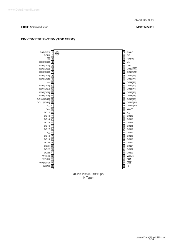
- Package: 70-pin 400 mil plastic TSOP (Type 2) (TSOP(2)70-P-400-0.50-K) (Product: MSM5424331TS-AK)