2N5191G Datasheet Text
2N5190G, 2N5191G, 2N5192G Silicon NPN Power Transistors
Silicon NPN power transistors are for use in power amplifier and switching circuits,
- excellent safe area limits. plement to PNP 2N5194, 2N5195.
Features http://onsemi.
- Epoxy Meets UL 94 V- 0 @ 0.125 in.
- These Devices are Pb- Free and are RoHS pliant-
MAXIMUM RATINGS
Rating Collector- Emitter Voltage 2N5190G 2N5191G 2N5192G Collector- Base Voltage 2N5190G 2N5191G 2N5192G Emitter- Base Voltage Collector Current Base Current Total Device Dissipation @ TC = 25°C Derate above 25°C Operating and Storage Junction Temperature Range ESD
- Human Body Model ESD
- Machine Model Symbol VCEO 40 60 80 VCBO 40 60 80 VEBO IC IB PD 40 320 TJ, Tstg HBM MM
- 65 to +150 3B C W mW/°C °C V V 5.0 4.0 1.0 Vdc Adc Adc Vdc Value Unit Vdc
4.0 AMPERES NPN SILICON POWER TRANSISTORS 40, 60, 80 VOLTS
- 40 WATTS
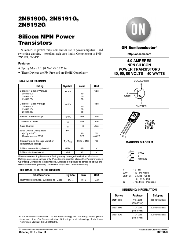
COLLECTOR 2
3 BASE 1 EMITTER
TO- 225 CASE 77 STYLE 1 1 2 3
MARKING DIAGRAM
Stresses exceeding Maximum Ratings may damage the device. Maximum Ratings are stress ratings only. Functional operation above the Remended Operating Conditions is not implied. Extended exposure to stresses above the Remended Operating Conditions may affect device reliability.
YWW 2 N519xG
THERMAL CHARACTERISTICS
Characteristic Thermal Resistance, Junction- to- Case Symbol RqJC Max 3.12 Unit °C/W
Y = Y ear WW = W ork Week 2N519x = Device Code x = 0, 1, or 2 G = Pb- Free Package
ORDERING INFORMATION
Device 2N5190G 2N5191G 2N5192G Package TO- 225 (Pb- Free) TO- 225 (Pb- Free) TO- 225 (Pb- Free) Shipping 500 Units/Box 500 Units/Box 500 Units/Box
- For additional information on our Pb- Free strategy and soldering details, please download the ON Semiconductor Soldering and Mounting Techniques Reference Manual, SOLDERRM/D.
© Semiconductor ponents...