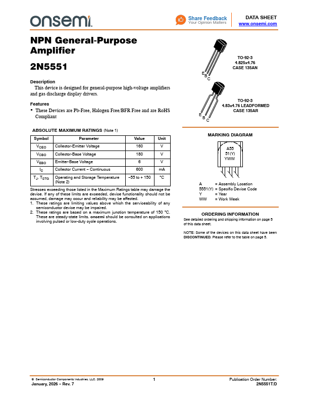
2N5551
Description
This device is designed for general-purpose high-voltage amplifiers and gas discharge display drivers.
Features
- These Devices are Pb-Free, Halogen Free/BFR Free and are Ro HS pliant
ABSOLUTE MAXIMUM RATINGS (Note 1)
Symbol
Parameter
Value
Unit
VCEO VCBO VEBO
IC TJ, TSTG
Collector-Emitter Voltage Collector-Base Voltage Emitter-Base Voltage Collector Current
- Continuous Operating and Storage Temperature (Note 2)
600 m A
- 55 to + 150 C
Stresses exceeding those listed in the Maximum Ratings table may damage the device. If any of these limits are exceeded, device functionality should not be assumed, damage may occur and reliability may be affected. 1. These ratings are limiting values above which the serviceability of any semiconductor device may be impaired. 2. These ratings are based on a maximum junction temperature of 150 C.
These are steady-state limits. onsemi should be consulted on applications involving pulsed or low-duty cycle...