2SJ665 Description
EN8590A 2SJ665 P-Channel Power MOSFET 100V, 27A, 77mΩ, TO-263-2L http://onsemi.
2SJ665 Key Features
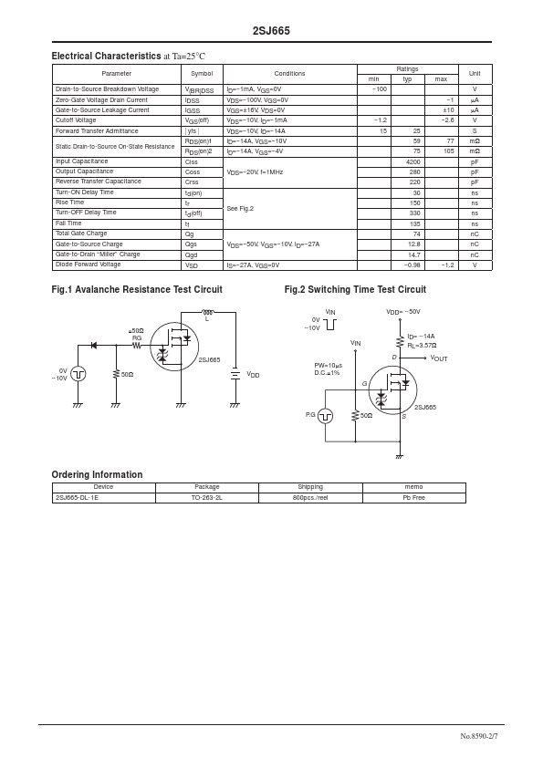
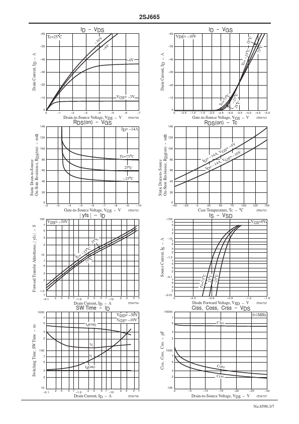
- ON-resistance RDS(on)1=59mΩ(typ.)
- 4V drive
- Input capacitance Ciss=4200pF (typ.)
2SJ665 is P-Channl Silicon MOSFET manufactured by onsemi .
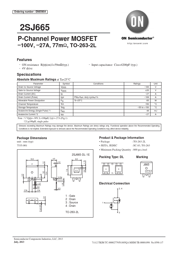
EN8590A 2SJ665 P-Channel Power MOSFET 100V, 27A, 77mΩ, TO-263-2L http://onsemi.