logo

ASM3P622S00E Datasheet, ON Semiconductor

ASM3P622S00E ic equivalent, low frequency peak emi reduction ic.

ASM3P622S00E Avg. rating / M : 1.0 rating-17

datasheet Download

ASM3P622S00E Datasheet

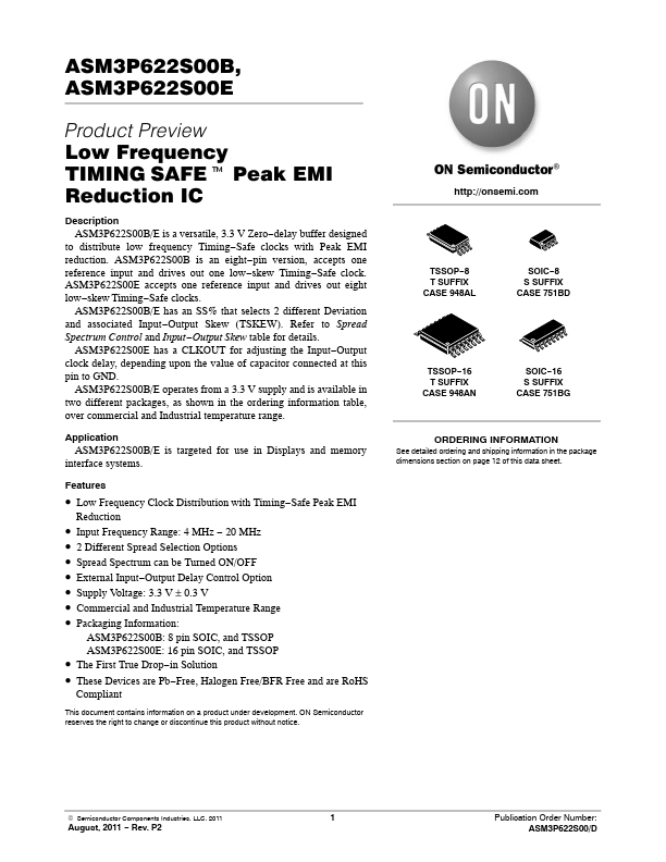
Features and benefits


* Low Frequency Clock Distribution with Timing−Safe Peak EMI Reduction
* Input Frequency Range: 4 MHz − 20 MHz
* 2 Different Spread Selection Options
* Sp.

Application

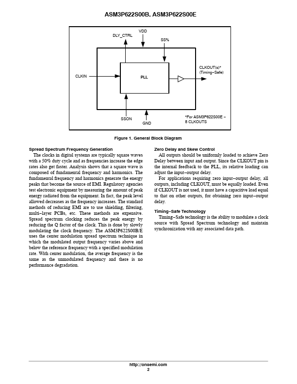
requiring zero input−output delay, all outputs, including CLKOUT, must be equally loaded. Even if CLKOUT is not used, it.

Description

ASM3P622S00B/E is a versatile, 3.3 V Zero−delay buffer designed to distribute low frequency Timing−Safe clocks with Peak EMI reduction. ASM3P622S00B is an eight−pin version, accepts one reference input and drives out one low−skew Timing−Safe clock. A.

Image gallery

ASM3P622S00E Page 1 ASM3P622S00E Page 2 ASM3P622S00E Page 3

Since 2006. D4U Semicon.   |   Contact Us   |   Privacy Policy   |   Purchase of parts