Full PDF Text Transcription for BDC01D (Reference)
Note: Below is a high-fidelity text extraction (approx. 800 characters) for
BDC01D. For precise diagrams, and layout, please refer to the original PDF.
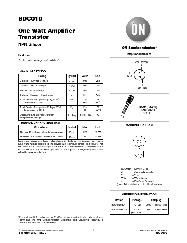
BDC01D One Watt Amplifier Transistor NPN Silicon Features • Pb−Free Package is Available* MAXIMUM RATINGS Rating Symbol Value Unit Collector −Emitter Voltage Collector −B...
View more extracted text
TINGS Rating Symbol Value Unit Collector −Emitter Voltage Collector −Base Voltage Emitter −Base Voltage Collector Current − Continuous Total Device Dissipation @ TA = 25°C Derate above 25°C VCEO VCBO VEBO IC PD 100 Vdc 100 Vdc 5.0 Vdc 0.5 Adc 1.0 W 8.0 mW/°C Total Device Dissipation @ TC = 25°C Derate above 25°C PD 2.5 W 20 mW/°C Operating and Storage Junction Temperature Range TJ, Tstg −55 to +150 °C THERMAL CHARACTERISTICS Characteristic Symbol Max Unit Thermal Resistance, Junction−to−Ambient RqJA 125 °C/W Thermal Resistance, Junction−to−Case RqJC 50 °C/W Maximum ratings are those values beyond which device damage can oc