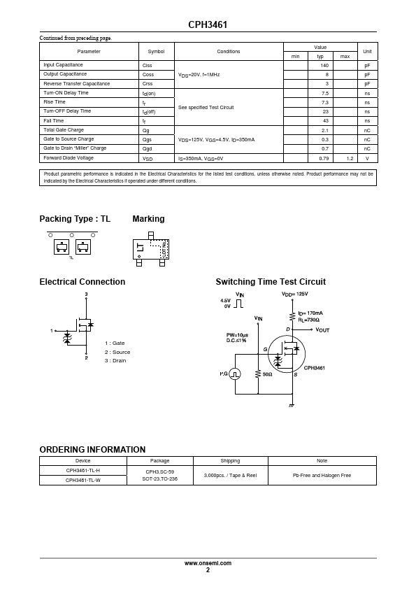
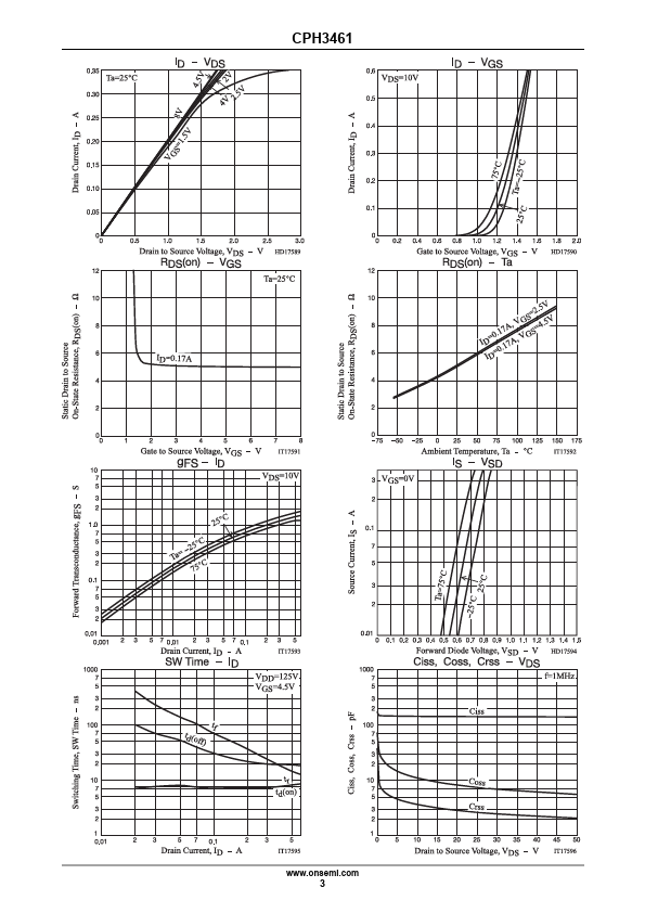
Low Ciss and High Speed Switching
Specifications
Absolute Maximum Ratings at Ta = 25C
Parameter
Symbol
Conditions
Drain to Source Voltage Gate to Source Voltage Drain to Gate Voltage Gate to Drain Voltage
VDSS VGSS VDGS VGDS
Drain Current (DC) Drain Current (Pulse) Power Dissipation Junction Temperature
ID IDP PW10s, duty cycle1% PD When moun.
Full PDF Text Transcription for CPH3461 (Reference)
Note: Below is a high-fidelity text extraction (approx. 800 characters) for
CPH3461. For precise diagrams, and layout, please refer to the original PDF.
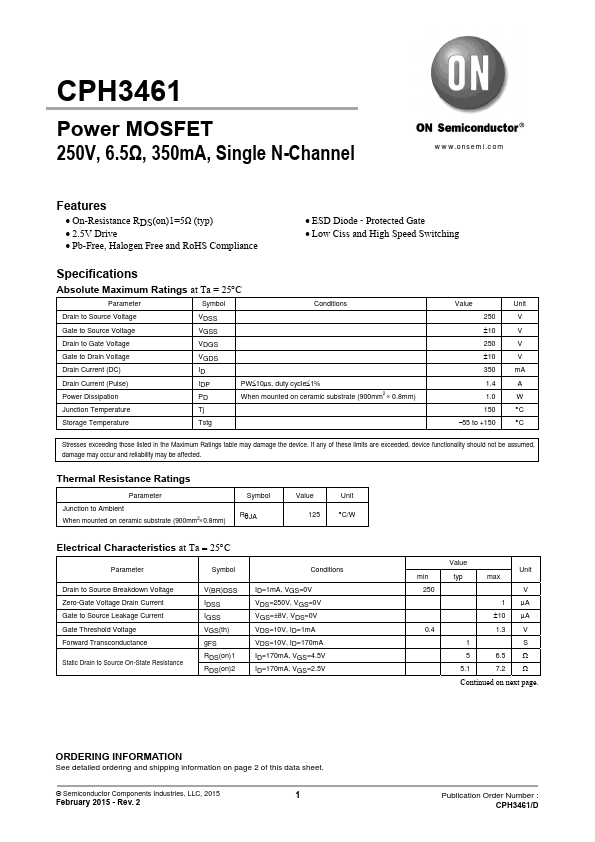
CPH3461 Power MOSFET 250V, 6.5Ω, 350mA, Single N-Channel www.onsemi.com Features On-Resistance RDS(on)1=5Ω (typ) 2.5V Drive Pb-Free, Halogen Free and RoHS Complianc...
View more extracted text
(on)1=5Ω (typ) 2.5V Drive Pb-Free, Halogen Free and RoHS Compliance ESD Diode - Protected Gate Low Ciss and High Speed Switching Specifications Absolute Maximum Ratings at Ta = 25C Parameter Symbol Conditions Drain to Source Voltage Gate to Source Voltage Drain to Gate Voltage Gate to Drain Voltage VDSS VGSS VDGS VGDS Drain Current (DC) Drain Current (Pulse) Power Dissipation Junction Temperature ID IDP PW10s, duty cycle1% PD When mounted on ceramic substrate (900mm2 0.8mm) Tj Storage Temperature Tstg Value 250 10 250 10 350 1.4 1.0 150 55 to +150 Unit V V V V mA A W C C Stresses exceeding those listed i