Optimal for load switch use (N-Channel for drive is embedded).
N-Channel : 1.5V drive, P-Channel : 1.8V drive.
Halogen Free compliance
Specifications
Absolute Maximum Ratings at Ta=25°C
Parameter
Symbol
Conditions
Drain to Source Voltage Gate to Source Voltage Drain Current (DC) Drain Current (Pulse) Allowable Power Dissipation Channel Temperature
VDSS VGSS ID IDP PD Tch
PW≤10μ.
Full PDF Text Transcription for CPH6635 (Reference)
Note: Below is a high-fidelity text extraction (approx. 800 characters) for
CPH6635. For precise diagrams, and layout, please refer to the original PDF.
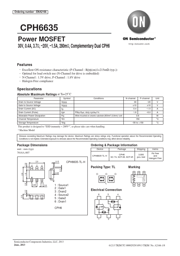
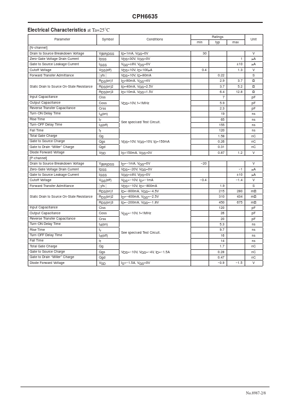
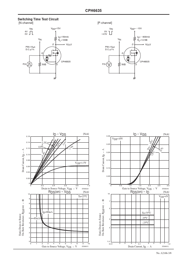
Ordering number : ENA2166 CPH6635 Power MOSFET 30V, 0.4A, 3.7Ω, –20V, –1.5A, 280mΩ, Complementary Dual CPH6 http://onsemi.com Features • Excellent ON-resistance character...
View more extracted text
al CPH6 http://onsemi.com Features • Excellent ON-resistance characteristic (P-Channel : RDS(on)1=215mΩ (typ.)) • Optimal for load switch use (N-Channel for drive is embedded) • N-Channel : 1.5V drive, P-Channel : 1.8V drive • Halogen Free compliance Specifications Absolute Maximum Ratings at Ta=25°C Parameter Symbol Conditions Drain to Source Voltage Gate to Source Voltage Drain Current (DC) Drain Current (Pulse) Allowable Power Dissipation Channel Temperature VDSS VGSS ID IDP PD Tch PW≤10μs, duty cycle≤1% When mounted on ceramic substrate (900mm2×0.8mm) 1unit Storage Temperature Tstg This product is designed to “ESD immun