FAN3121
FAN3121 is Low-Side Gate Driver manufactured by onsemi.
Description
The FAN3121 and FAN3122 MOSFET drivers are designed to drive
N- channel enhancement MOSFETs in low- side switching applications by providing high peak current pulses. The drivers are available with either TTL input thresholds (FAN312x T) or VDD- proportional CMOS input thresholds (FAN312x C). Internal circuitry provides an under- voltage lockout function by holding the output low until the supply voltage is within the operating range.
FAN312x drivers incorporate the Miller Drive™ architecture for the final output stage. This bipolar / MOSFET bination provides the highest peak current during the Miller plateau stage of the MOSFET turn- on / turn- off process.
The FAN3121 and FAN3122 drivers implement an enable function on pin 3 (EN), previously unused in the industry- standard pin- out. The pin is internally pulled up to VDD for active HIGH logic and can be left open for standard operation.
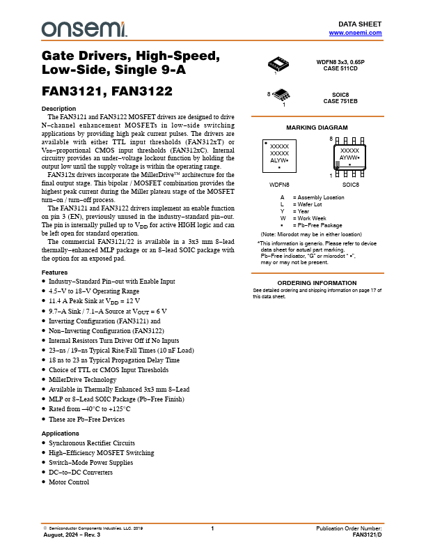
The mercial FAN3121/22 is available in a 3x3 mm 8- lead thermally- enhanced MLP package or an 8- lead SOIC package with the option for an exposed pad.
Features
- Industry- Standard Pin- out with Enable Input
- 4.5- V to 18- V Operating Range
- 11.4 A Peak Sink at VDD = 12 V
- 9.7- A Sink / 7.1- A Source at VOUT = 6 V
- Inverting Configuration (FAN3121) and
- Non- Inverting Configuration (FAN3122)
- Internal Resistors Turn Driver Off if No Inputs
- 23- ns / 19- ns Typical Rise/Fall Times (10 n F Load)
- 18 ns to 23 ns Typical Propagation Delay Time
- Choice of TTL or CMOS Input Thresholds
- Miller Drive Technology
- Available in Thermally Enhanced 3x3 mm 8- Lead
- MLP or 8- Lead SOIC Package (Pb- Free Finish)
- Rated from
- 40°C to +125°C
- These are Pb- Free Devices
Applications
- Synchronous Rectifier Circuits
- High- Efficiency MOSFET Switching
- Switch- Mode Power Supplies
- DC- to- DC Converters
- Motor Control
DATA SHEET .onsemi.
WDFN8 3x3, 0.65P CASE 511CD
8 1
SOIC8 CASE 751EB
MARKING DIAGRAM
XXXXX XXXXX ALYWG
WDFN8
XXXXX...