FDD6N50TM-F085
Features
- 6A, 500V, RDS(on) = 0.9Ω @VGS = 10 V
- Low gate charge ( typical 12.8 n C)
- Low Crss ( typical 9 p F)
- Fast switching
- 100% avalanche tested
- Improved dv/dt capability
- Qualified to AEC Q101
- Ro HS pliant
Description
These N-Channel enhancement mode power field effect transistors are produced using ON Semiconductor's proprietary, planar stripe, DMOS technology. This advanced technology has been especially tailored to minimize on-state resistance, provide superior switching performance, and withstand high energy pulse in the avalanche and mutation mode. These devices are well suited for high efficient switched mode power supplies and active power factor correction.
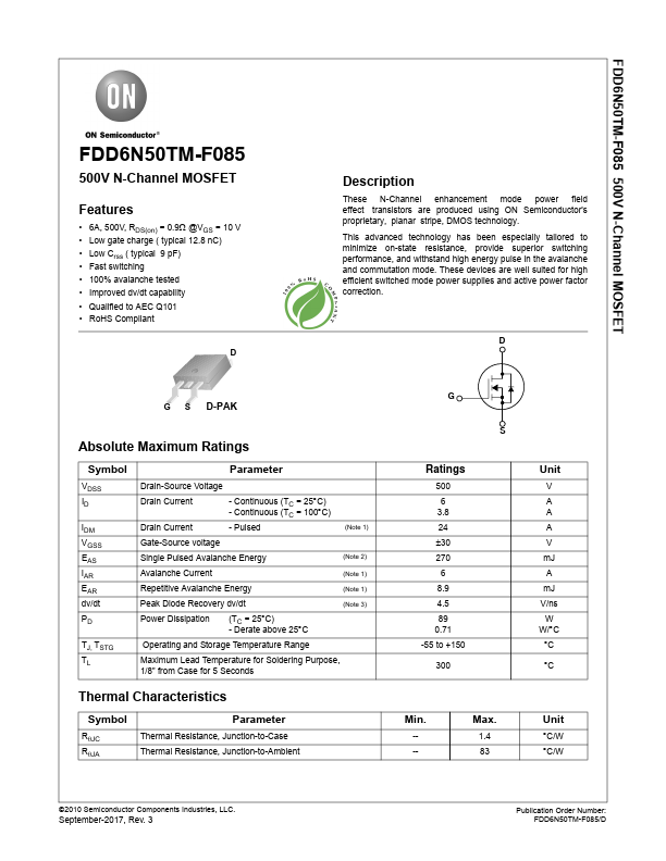
G S D-PAK
Absolute Maximum Ratings
Symbol
VDSS ID
IDM VGSS EAS IAR EAR dv/dt PD
TJ, TSTG TL
Parameter
Drain-Source Voltage
Drain Current Drain Current
- Continuous (TC = 25°C)
- Continuous (TC = 100°C)
- Pulsed
(Note 1)
Gate-Source voltage
Single Pulsed Avalanche Energy
(Note 2)
Avalanche...