FDV301N-F169
FDV301N-F169 is N-Channel Digital FET manufactured by onsemi.
- Part of the FDV301N comparator family.
- Part of the FDV301N comparator family.
Digital FET, N-Channel
FDV301N, FDV301N-F169
General Description This N- Channel logic level enhancement mode field effect transistor is produced using onsemi’s proprietary, high cell density, DMOS technology. This very high density process is especially tailored to minimize on- state resistance. This device has been designed especially for low voltage applications as a replacement for digital transistors. Since bias resistors are not required, this one N- channel FET can replace several different digital transistors, with different bias resistor values.
Features
- 25 V, 0.22 A Continuous, 0.5 A Peak
- RDS(on) = 5 W @ VGS = 2.7 V
- RDS(on) = 4 W @ VGS = 4.5 V
- Very Low Level Gate Drive Requirements Allowing Direct
Operation in 3 V Circuits. VGS(th) < 1.06 V
- Replace Multiple NPN Digital Transistors with One DMOS FET
- This Device is Pb- Free and Halide Free
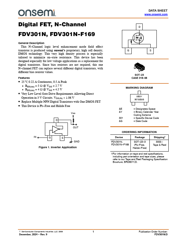
Vcc
Figure 1. Inverter Application
DATA SHEET .onsemi.
SOT- 23 CASE 318- 08
MARKING DIAGRAM
&E&Y 301&E&G
&E
= Designates Space
&Y
= Binary Calendar Year
Coding Scheme
= Specific Device Code
&G
= Date Code
ORDERING INFORMATION
Device
Package
Shipping†
FDV301N, FDV301N-...