FQA11N90C-F109
Features
- 11 A, 900 V, RDS(on) = 1.1 Ω (Max.) @ VGS = 10 V, ID = 5.5 A
- Low Gate Charge (Typ. 60 n C)
- Low Crss (Typ. 23 p F)
- 100% Avalanche Tested
- Ro HS pliant
Description
This N-Channel enhancement mode power MOSFET is produced using ON Semiconductor’s proprietary planar stripe and DMOS technology. This advanced MOSFET technology has been especially tailored to reduce on-state resistance, and to provide superior switching performance and high avalanche energy strength. These devices are suitable for switched mode power supplies, active power factor correction (PFC), and elec-tronic lamp ballasts.
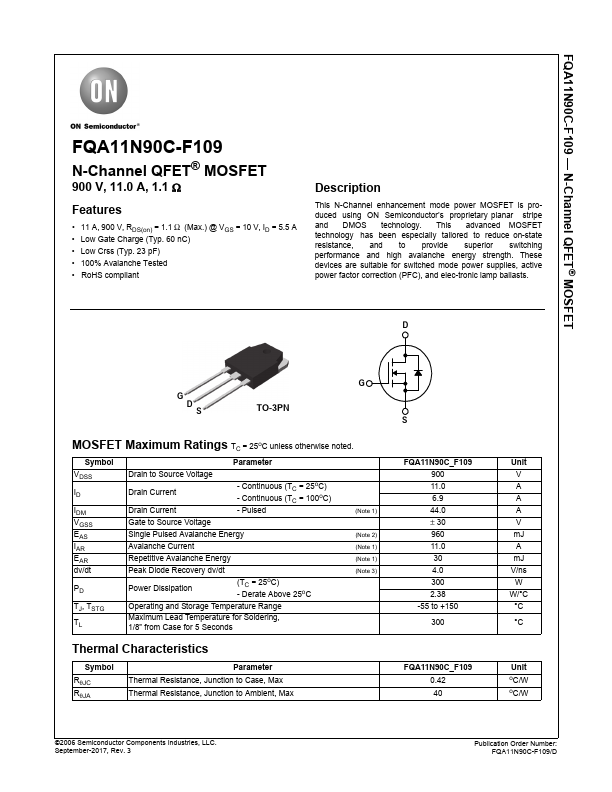
TO-3PN
MOSFET Maximum Ratings TC = 25o C unless otherwise noted.
Symbol VDSS
IDM VGSS EAS IAR EAR dv/dt
TJ, TSTG
Parameter
Drain to Source Voltage Drain Current Drain Current
- Continuous (TC = 25o C)
- Continuous (TC = 100o C)
- Pulsed
Gate to Source Voltage
Single Pulsed Avalanche Energy
Avalanche Current
Repetitive Avalanche Energy
Peak Diode Recovery...