Datasheet4U Logo Datasheet4U.com

FSA557 Datasheet Low Supply Signal Bypass-IC

Manufacturer: onsemi

General Description

Pin No.

WLCSP12 Pin Name Description 
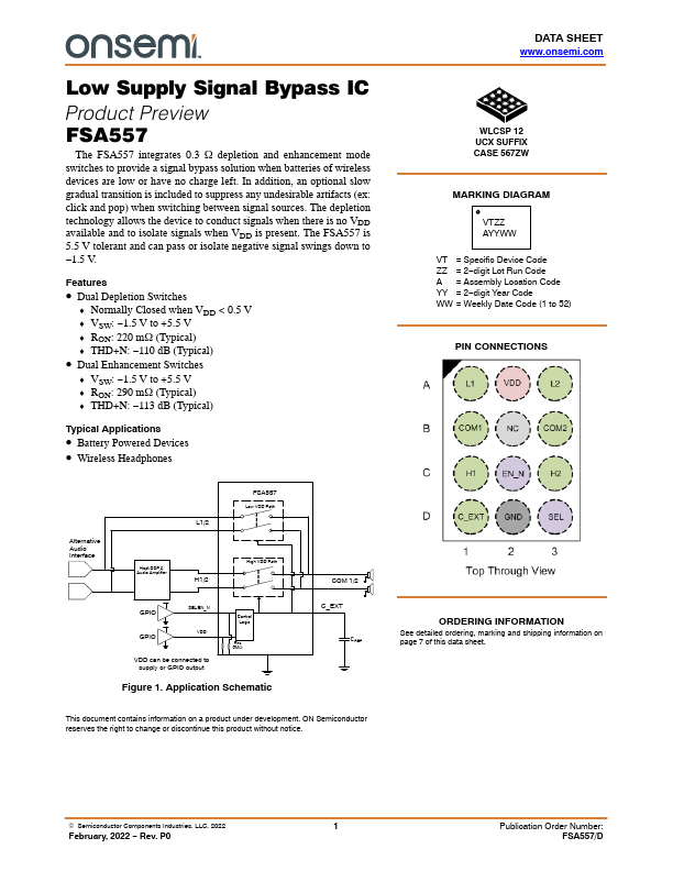
A1 L1 Low Supply Signal Path 1 A2 VDD Power Supply or Select Signal from Host GPIO A3 L2 Low Supply Signal Path 2

Overview

Low Supply Signal Bypass IC Product Preview FSA557 The FSA557 integrates 0.3 W depletion and enhancement mode switches to provide a signal bypass solution when batteries of wireless devices are low or have no charge left.

In addition, an optional slow gradual transition is included to suppress any undesirable artifacts (ex: click and pop) when switching between signal sources.

The depletion technology allows the device to conduct signals when there is no VDD available and to isolate signals when VDD is present.

Key Features

  • Dual Depletion Switches.
  • Normally Closed when VDD < 0.5 V.
  • VSW:.
  • 1.5 V to +5.5 V.
  • RON: 220 mW (Typical).
  • THD+N:.
  • 110 dB (Typical).
  • Dual Enhancement Switches.
  • VSW:.
  • 1.5 V to +5.5 V.
  • RON: 290 mW (Typical).
  • THD+N:.
  • 113 dB (Typical) Typical.