HGTG12N60A4D Overview
Key Specifications
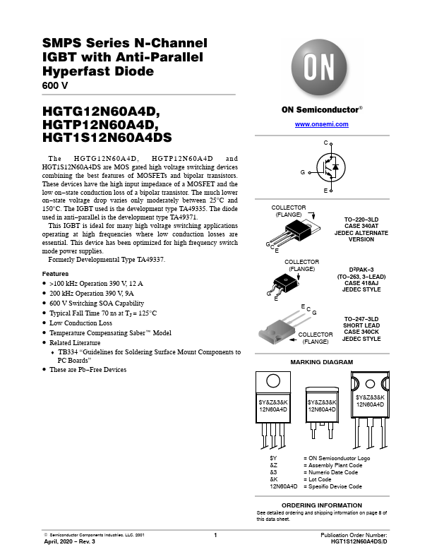
Package: TO-247-3
Mount Type: Through Hole
Pins: 3
Height: 4.82 mm
Key Features
- >100 kHz Operation 390 V, 12 A
- 200 kHz Operation 390 V, 9A
- 600 V Switching SOA Capability
- Typical Fall Time 70 ns at TJ = 125°C
- Low Conduction Loss