J113
Overview
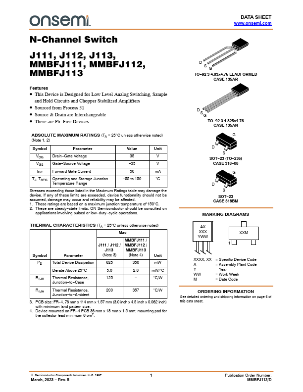
- This Device is Designed for Low Level Analog Switching, Sample and Hold Circuits and Chopper Stabilized Amplifiers
- Sourced from Process 51
- Source & Drain are Interchangeable
- These are Pb-Free Devices
| Part | J113 |
|---|---|
| Description | N-Channel Switch |
| Manufacturer | onsemi |
| Size | 322.12 KB |
| Part Number | Manufacturer | Description |
|---|---|---|
| J113 | InterFET | N-Channel JFET |
| J113 | Fairchild Semiconductor | N-Channel Switch |
| J113 | Vishay | N-Channel JFETs |
| J113 | Motorola Semiconductor | JFET CHOPPER |
| J113 | NXP Semiconductors | N-channel silicon field-effect transistors |