LC898212XD Description
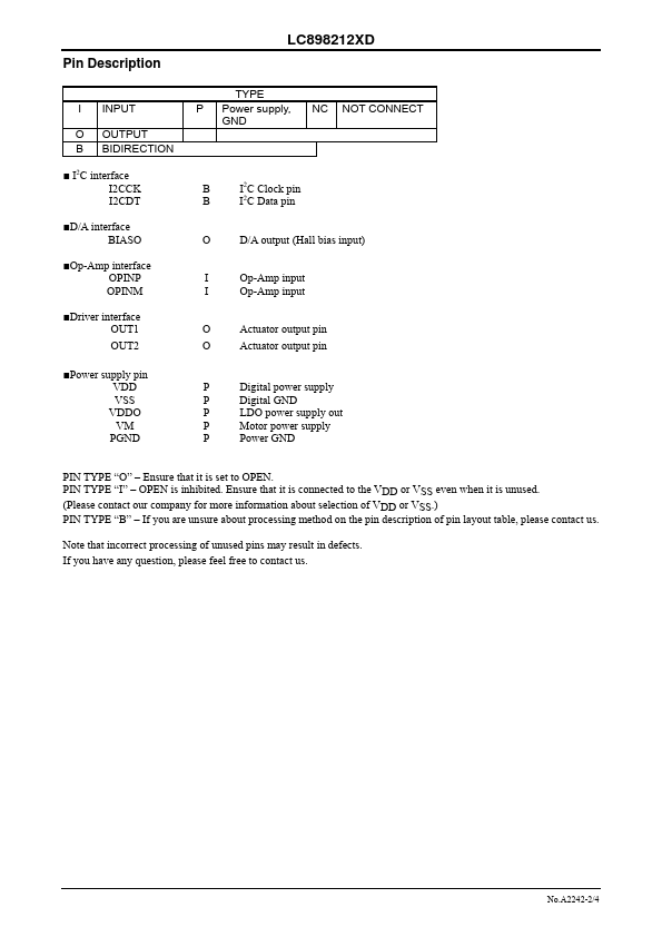
I INPUT O OUTPUT B BIDIRECTION I2C interface I2CCK I2CDT D/A interface BIASO Op-Amp interface OPINP OPINM Driver interface OUT1 OUT2 Power supply pin VDD VSS VDDO VM PGND LC898212XD TYPE P Power supply, GND NC NOT CONNECT B I2C Clock pin B I2C Data pin O D/A output (Hall bias input) I Op-Amp input I Op-Amp input O Actuator output pin O Actuator output pin P Digital power supply P Digital GND P LDO power supply out P...
LC898212XD Key Features
- AF control equalize circuit
- Any coefficient can be specified by I2C I/F
- Maximum 10-bit
- Input 2 channel
- Output 2-channel (Hall offset, Constant current Bias)
- 1 channel
- Hall Amp
- 48MHz (Frequency adjustment function)
- PWM circuit for AF control
- Saturation drive H bridge 1 channel