MC10121
Overview
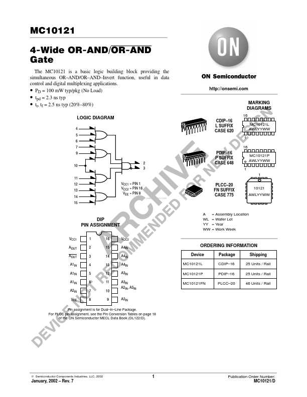
MC10121 4-Wide OR-AND/OR-AND Gate The MC10121 is a basic logic building block providing the simultaneous OR–AND/OR–AND–Invert function, useful in data control and digital multiplexing applications. • ...
| Part | MC10121 |
|---|---|
| Description | 4-Wide OR-AND/OR-AND Gate |
| Manufacturer | onsemi |
| Size | 134.50 KB |
MC10121 4-Wide OR-AND/OR-AND Gate The MC10121 is a basic logic building block providing the simultaneous OR–AND/OR–AND–Invert function, useful in data control and digital multiplexing applications. • ...
| Part Number | Manufacturer | Description |
|---|---|---|
| MC10121 | Motorola Semiconductor | 4-Wide OR-AND/OR-AND Gate |
| MC10124 | Motorola Semiconductor | Quad TTL to MECL Translator |
| MC10129 | Motorola Semiconductor | Quad Bus Receiver |
| MC10123 | Motorola Semiconductor | Triple 4-3-3-Input Bus Driver |
| MC10125 | Motorola Semiconductor | Quad MECL to TTL Transistor |