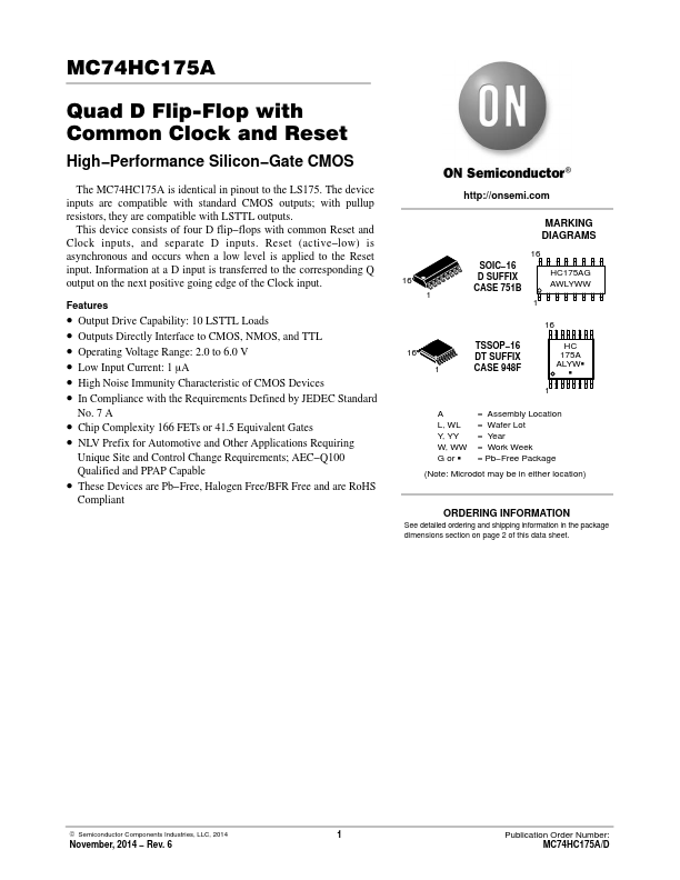
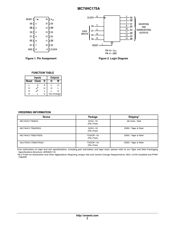
Datasheet4U Logo Datasheet4U.com

MC74HC175A - Quad D Flip-Flop

Features

  • Output Drive Capability: 10 LSTTL Loads.
  • Outputs Directly Interface to CMOS, NMOS, and TTL.
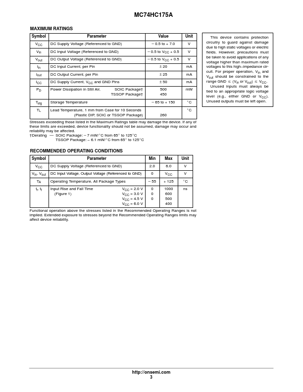
  • Operating Voltage Range: 2.0 to 6.0 V.
  • Low Input Current: 1 mA.
  • High Noise Immunity Characteristic of CMOS Devices.
  • In Compliance with the Requirements Defined by JEDEC Standard No. 7 A.
  • Chip Complexity 166 FETs or 41.5 Equivalent Gates.
  • NLV Prefix for Automotive and Other.

📥 Download Datasheet

Full PDF Text Transcription (Reference)

The following content is an automatically extracted verbatim text from the original manufacturer datasheet and is provided for reference purposes only.

View original datasheet text
MC74HC175A Quad D Flip-Flop with Common Clock and Reset High−Performance Silicon−Gate CMOS The MC74HC175A is identical in pinout to the LS175. The device inputs are compatible with standard CMOS outputs; with pullup resistors, they are compatible with LSTTL outputs. This device consists of four D flip−flops with common Reset and Clock inputs, and separate D inputs. Reset (active−low) is asynchronous and occurs when a low level is applied to the Reset input. Information at a D input is transferred to the corresponding Q output on the next positive going edge of the Clock input. Features • Output Drive Capability: 10 LSTTL Loads • Outputs Directly Interface to CMOS, NMOS, and TTL • Operating Voltage Range: 2.0 to 6.
Published: |