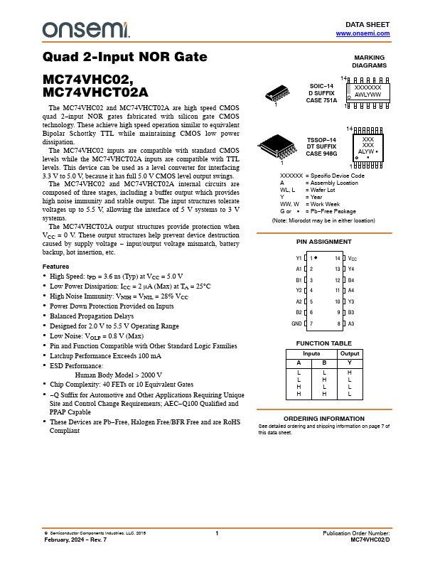
MC74VHC02 Overview
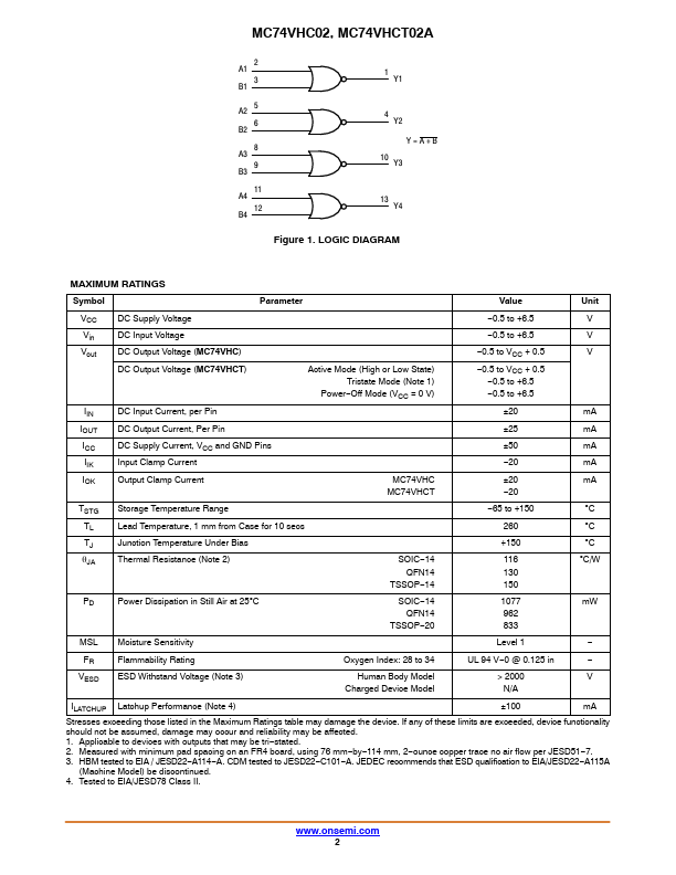
Quad 2-Input NOR Gate MC74VHC02, MC74VHCT02A The MC74VHC02 and MC74VHCT02A are high speed CMOS quad 2−input NOR gates fabricated with silicon gate CMOS technology. These achieve high speed operation similar to equivalent Bipolar Schottky TTL while maintaining CMOS low power dissipation. The MC74VHC02 inputs are patible with standard CMOS levels while the MC74VHCT02A inputs are patible with TTL levels.
MC74VHC02 Key Features
- High Speed: tPD = 3.6 ns (Typ) at VCC = 5.0 V
- Low Power Dissipation: ICC = 2 mA (Max) at TA = 25C
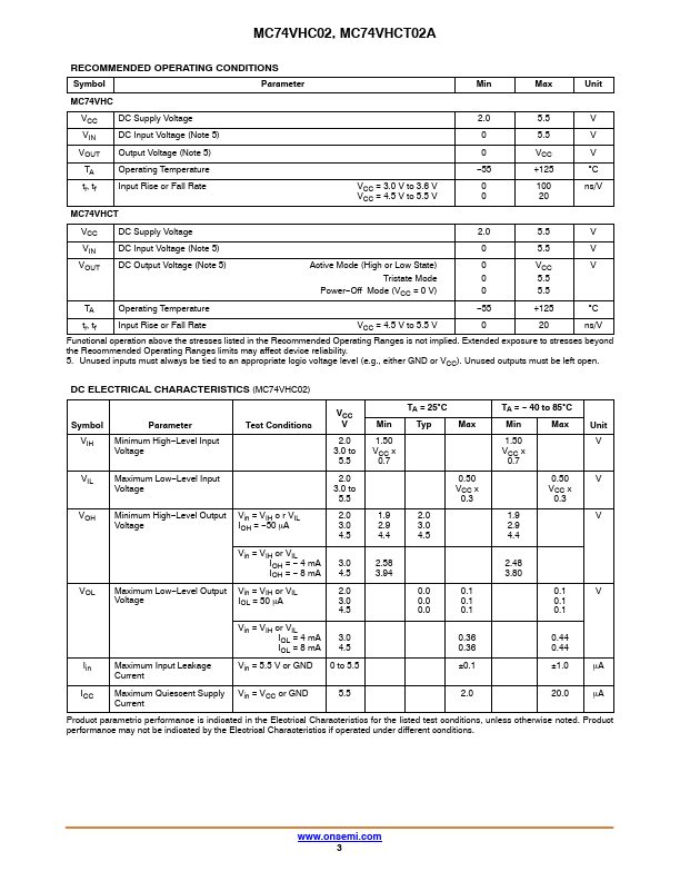
- High Noise Immunity: VNIH = VNIL = 28% VCC
- Power Down Protection Provided on Inputs
- Balanced Propagation Delays
- Designed for 2.0 V to 5.5 V Operating Range
- Low Noise: VOLP = 0.8 V (Max)
- Pin and Function patible with Other Standard Logic Families
- Latchup Performance Exceeds 100 mA
- ESD Performance