Datasheet4U Logo Datasheet4U.com

MC74VHC1GT07 - Single Non-Inverting Buffer

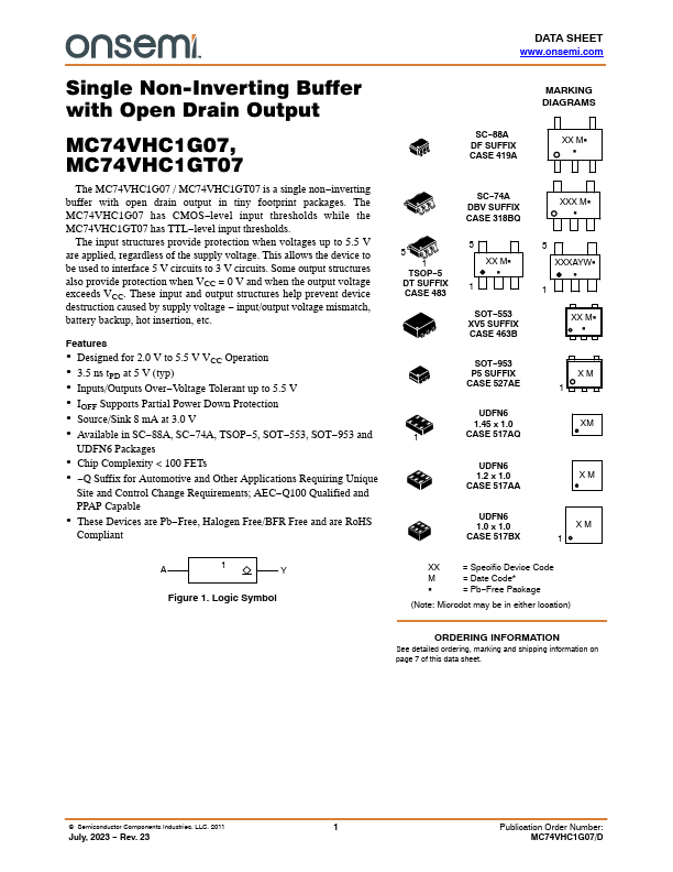
This page provides the datasheet information for the MC74VHC1GT07, a member of the MC74VHC1G07 Single Non-Inverting Buffer family.

Datasheet Summary

Features

  • Designed for 2.0 V to 5.5 V VCC Operation.
  • 3.5 ns tPD at 5 V (typ).
  • Inputs/Outputs Over.
  • Voltage Tolerant up to 5.5 V.
  • IOFF Supports Partial Power Down Protection.
  • Source/Sink 8 mA at 3.0 V.
  • Available in SC.
  • 88A, SC.
  • 74A, TSOP.
  • 5, SOT.
  • 553, SOT.
  • 953 and UDFN6 Packages.
  • Chip Complexity < 100 FETs.
  • Q Suffix for Automotive and Other.

📥 Download Datasheet

Datasheet preview – MC74VHC1GT07

Datasheet Details

Part number MC74VHC1GT07
Manufacturer ON Semiconductor
File Size 174.91 KB
Description Single Non-Inverting Buffer
Datasheet download datasheet MC74VHC1GT07 Datasheet
Additional preview pages of the MC74VHC1GT07 datasheet.
Other Datasheets by ON Semiconductor

Full PDF Text Transcription

Click to expand full text
DATA SHEET www.onsemi.com Single Non-Inverting Buffer with Open Drain Output MC74VHC1G07, MC74VHC1GT07 The MC74VHC1G07 / MC74VHC1GT07 is a single non−inverting buffer with open drain output in tiny footprint packages. The MC74VHC1G07 has CMOS−level input thresholds while the MC74VHC1GT07 has TTL−level input thresholds. The input structures provide protection when voltages up to 5.5 V are applied, regardless of the supply voltage. This allows the device to be used to interface 5 V circuits to 3 V circuits. Some output structures also provide protection when VCC = 0 V and when the output voltage exceeds VCC. These input and output structures help prevent device destruction caused by supply voltage − input/output voltage mismatch, battery backup, hot insertion, etc.
Published: |