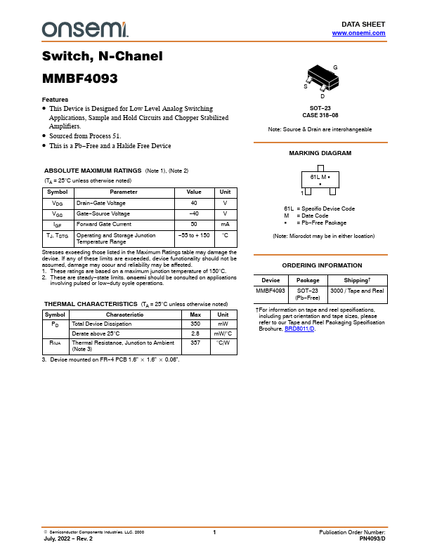
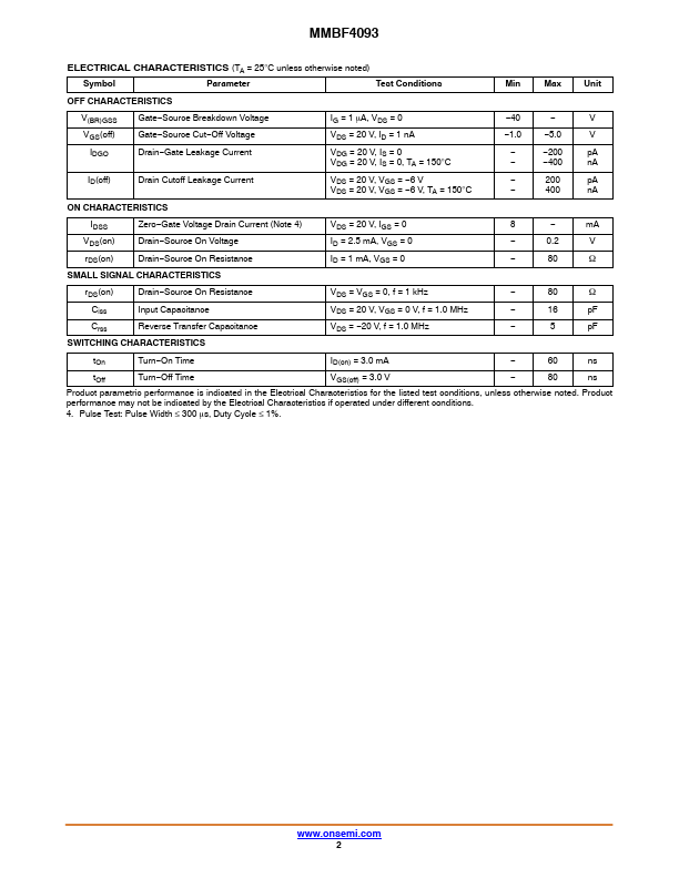
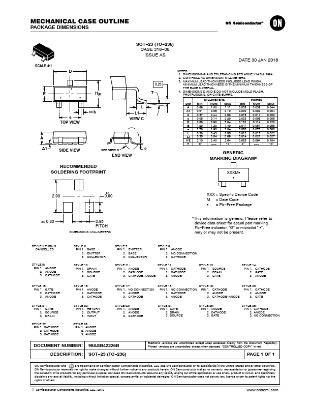
MMBF4093 Overview
Switch, N-Chanel MMBF4093.
MMBF4093 Key Features
- This Device is Designed for Low Level Analog Switching
MMBF4093 Applications
- Sourced from Process 51
| Part number | MMBF4093 |
|---|---|
| Datasheet | MMBF4093-ONSemiconductor.pdf |
| File Size | 145.19 KB |
| Manufacturer | onsemi |
| Description | N-Channel Switch |
|
|
Switch, N-Chanel MMBF4093.
| Brand Logo | Part Number | Description | Manufacturer |
|---|---|---|---|
| MMBF4093 | N-Channel Switch | Fairchild |