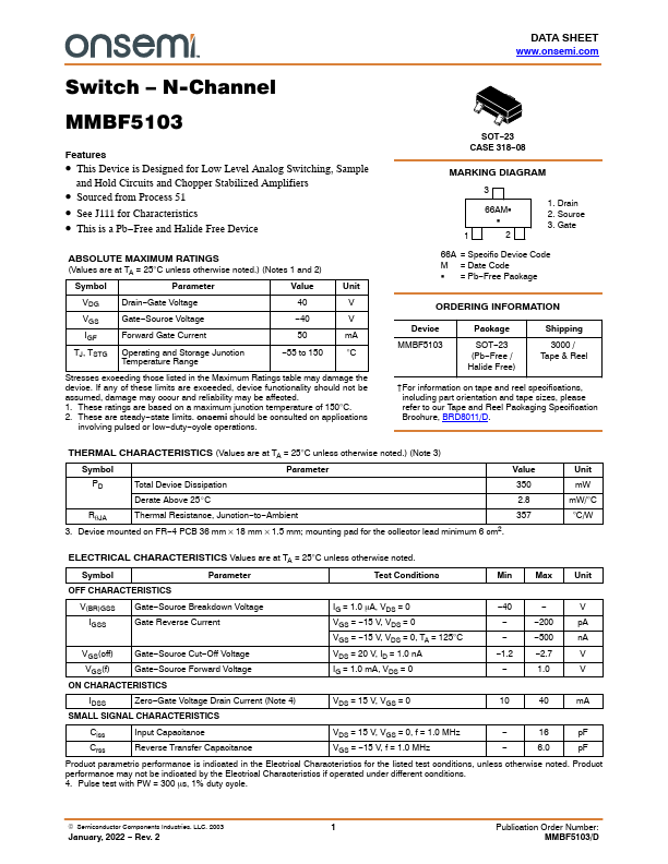
• Part: MMBF5103
  • Description: N-Channel Switch
  • Manufacturer: onsemi
  • Size: 141.93 KB
Download MMBF5103 Datasheet PDF
onsemi
MMBF5103
Features - This Device is Designed for Low Level Analog Switching, Sample and Hold Circuits and Chopper Stabilized Amplifiers - Sourced from Process 51 - See J111 for Characteristics - This is a Pb- Free and Halide Free Device ABSOLUTE MAXIMUM RATINGS (Values are at TA = 25°C unless otherwise noted.) (Notes 1 and 2) Symbol Parameter Value Unit Drain- Gate Voltage VGS IGF TJ, TSTG Gate- Source Voltage Forward Gate Current Operating and Storage Junction Temperature Range - 40 50 m A - 55 to 150 °C Stresses exceeding those listed in the Maximum Ratings table may damage the device. If any of these limits are exceeded, device functionality should not be assumed, damage may occur and reliability may be affected. 1. These ratings are based on a maximum junction temperature of 150°C. 2. These are steady- state limits. onsemi should be consulted on applications involving pulsed or low- duty- cycle operations. SOT- 23 CASE 318- 08 MARKING DIAGRAM 66AMG G 1. Drain...