MMBFJ110 Overview
Key Specifications
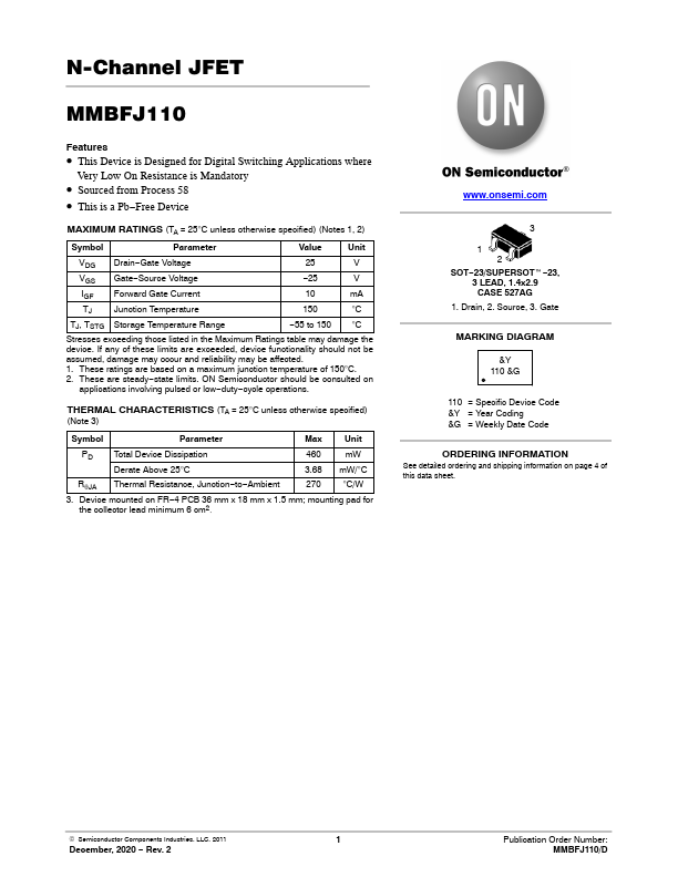
Package: SMD/SMT
Mount Type: Surface Mount
Pins: 3
Height: 1.12 mm
Key Features
- This Device is Designed for Digital Switching Applications where Very Low On Resistance is Mandatory
- Sourced from Process 58
- This is a Pb-Free Device