Full PDF Text Transcription for MPSW92 (Reference)
Note: Below is a high-fidelity text extraction (approx. 800 characters) for
MPSW92. For precise diagrams, and layout, please refer to the original PDF.
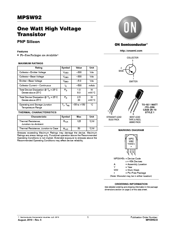
MPSW92 One Watt High Voltage Transistor PNP Silicon Features • Pb−Free Packages are Available* MAXIMUM RATINGS Rating Symbol Value Unit Collector −Emitter Voltage Collect...
View more extracted text
UM RATINGS Rating Symbol Value Unit Collector −Emitter Voltage Collector −Base Voltage Emitter −Base Voltage Collector Current − Continuous Total Device Dissipation @ TA = 25°C Derate above 25°C VCEO VCBO VEBO IC PD −300 −300 −5.0 −500 1.0 8.0 Vdc Vdc Vdc mAdc W mW/°C Total Device Dissipation @ TC = 25°C Derate above 25°C PD 2.5 W 20 mW/°C Operating and Storage Junction Temperature Range TJ, Tstg − 55 to +150 °C THERMAL CHARACTERISTICS Characteristic Symbol Max Unit Thermal Resistance, Junction−to−Ambient RqJA 125 °C/W Thermal Resistance, Junction to Case RqJC 50 °C/W Stresses exceeding Maximum Ratings may damage the devic