Full PDF Text Transcription for MSB710-RT1 (Reference)
Note: Below is a high-fidelity text extraction (approx. 800 characters) for
MSB710-RT1. For precise diagrams, and layout, please refer to the original PDF.
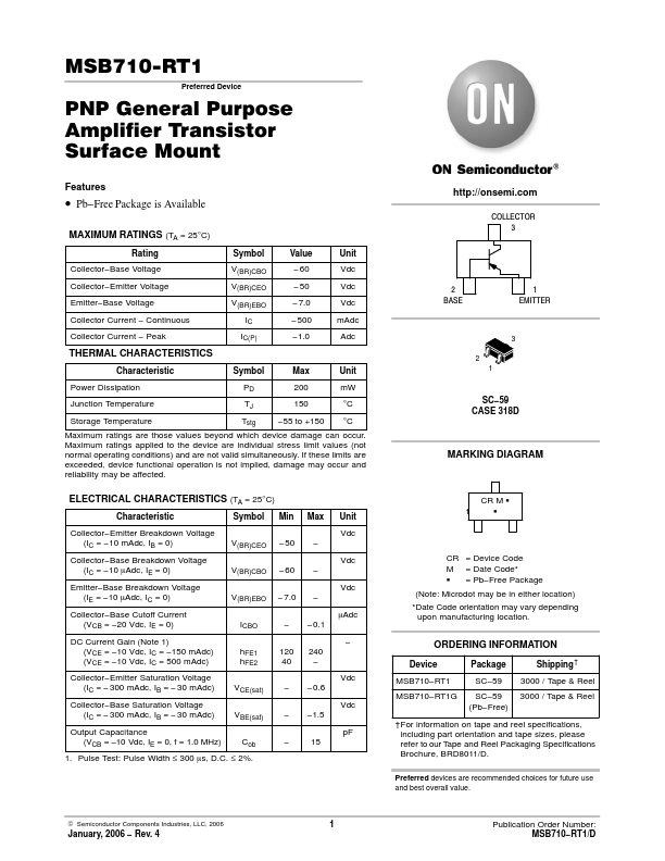
MSB710−RT1 Preferred Device PNP General Purpose Amplifier Transistor Surface Mount Features • Pb−Free Package is Available MAXIMUM RATINGS (TA = 25°C) Rating Collector−Ba...
View more extracted text
e Package is Available MAXIMUM RATINGS (TA = 25°C) Rating Collector−Base Voltage Collector−Emitter Voltage Emitter−Base Voltage Collector Current − Continuous Collector Current − Peak THERMAL CHARACTERISTICS Symbol V(BR)CBO V(BR)CEO V(BR)EBO IC IC(P) Value − 60 − 50 − 7.0 − 500 −1.0 Unit Vdc Vdc Vdc mAdc Adc Characteristic Symbol Max Unit Power Dissipation PD 200 mW Junction Temperature TJ 150 °C Storage Temperature Tstg −55 to +150 °C Maximum ratings are those values beyond which device damage can occur. Maximum ratings applied to the device are individual stress limit values (not normal operating conditions) and are not