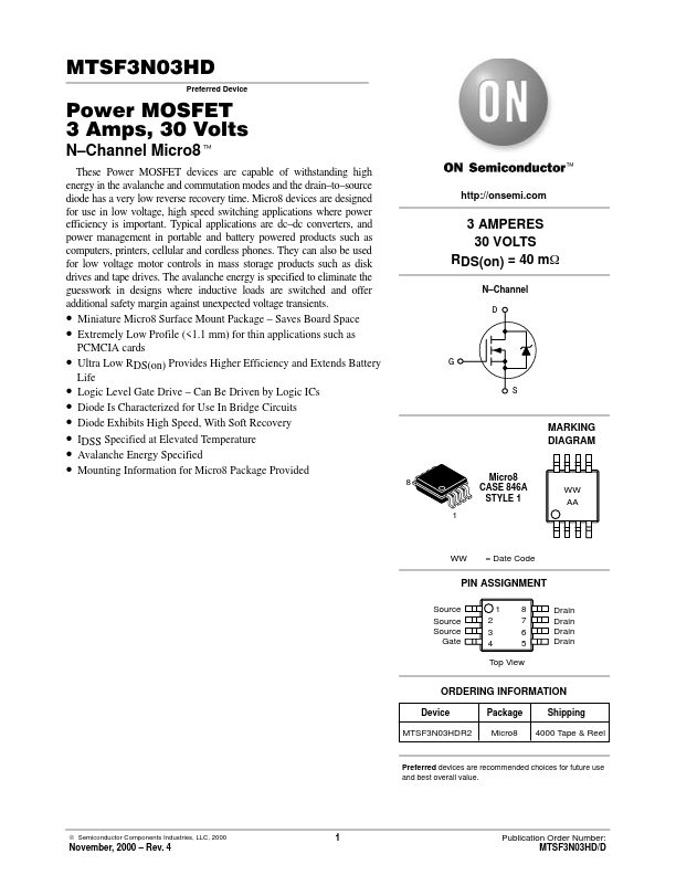
rdless of the switching speed. The circuit used to obtain the data is constructed to minimize common inductance in the drain and gate circuit loops and is believed readily achievable with board mounted components. Most power electronic loads are inductive; the data in the figure is taken with a resistive load, which approximates an optimally snubbed inductive load. Power MOSFETs may be safely operated into an inductive load; however, snubbing reduces switching losses. 1500 VDS = 0 V 1200 Ciss.
Full PDF Text Transcription for MTSF3N03HD (Reference)
Note: Below is a high-fidelity text extraction (approx. 800 characters) for
MTSF3N03HD. For precise diagrams, and layout, please refer to the original PDF.
MTSF3N03HD Preferred Device Power MOSFET 3 Amps, 30 Volts N–Channel Micro8t These Power MOSFET devices are capable of withstanding high energy in the avalanche and commut...
View more extracted text
es are capable of withstanding high energy in the avalanche and commutation modes and the drain–to–source diode has a very low reverse recovery time. Micro8 devices are designed for use in low voltage, high speed switching applications where power efficiency is important. Typical applications are dc–dc converters, and power management in portable and battery powered products such as computers, printers, cellular and cordless phones. They can also be used for low voltage motor controls in mass storage products such as disk drives and tape drives.