NB3H60113G Description
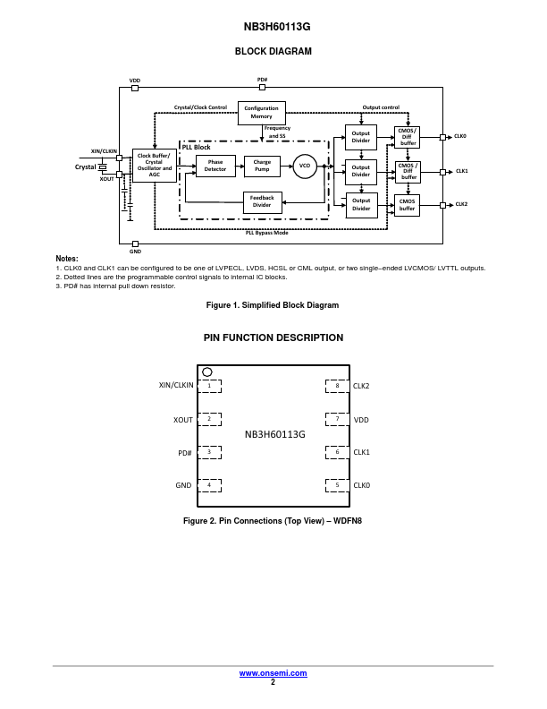
NB3H60113G 3.3 V / 2.5 V Programmable OmniClock Generator with Single Ended (LVCMOS/LVTTL) and Differential (LVPECL/LVDS/ HCSL/CML) Outputs .onsemi. The NB3H60113G, which is a member of the OmniClock family, is a one−time programmable (OTP), low power PLL−based clock generator that supports any output frequency from 8 kHz to 200 MHz. The device accepts fundamental mode parallel resonant crystal or a single ended...
NB3H60113G Key Features
- Member of the OmniClock Family of Programmable Clock
- Operating Power Supply: 3.3 V ± 10%, 2.5 V ± 10%
- I/O Standards
- Inputs: LVCMOS/LVTTL, Fundamental Mode Crystal
- Outputs: LVCMOS/LVTTL
- Outputs: LVPECL, LVDS, CML and HCSL
- 3 Programmable Single Ended (LVCMOS/LVTTL)
- Input Frequency Range
- Power Saving mode through Power Down Pin
- Programmable PLL Bypass Mode