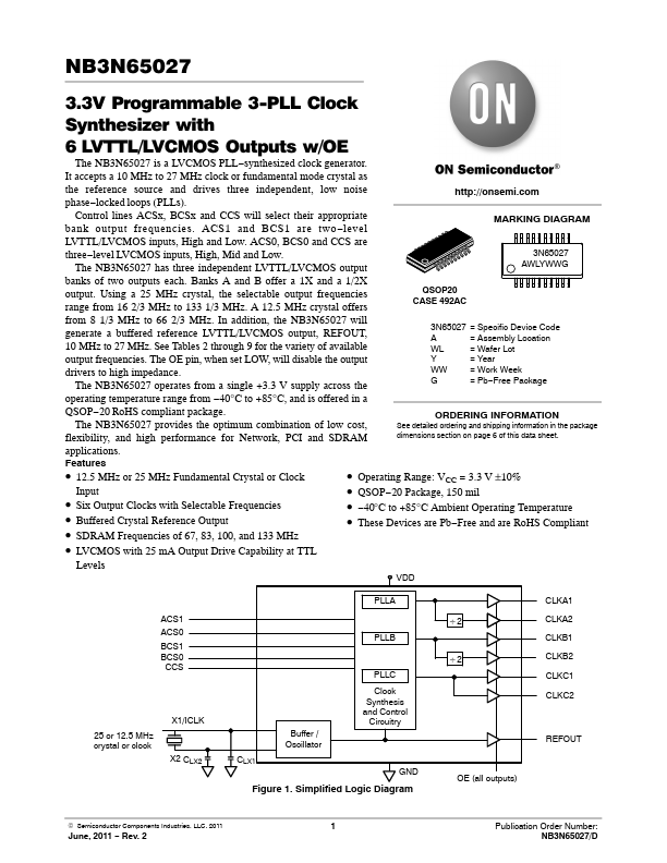
NB3N65027 Description
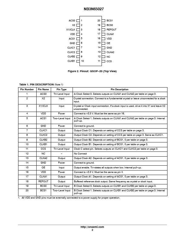
(Note 1) Pin Number Pin Name Pin Type Pin Description 1 ACS0 Tri−Level Input A Clock Select 0. Selects outputs on CLKA1 and CLKA2 per table on page 3. 2 X2 Input Crystal connection.
NB3N65027 Key Features
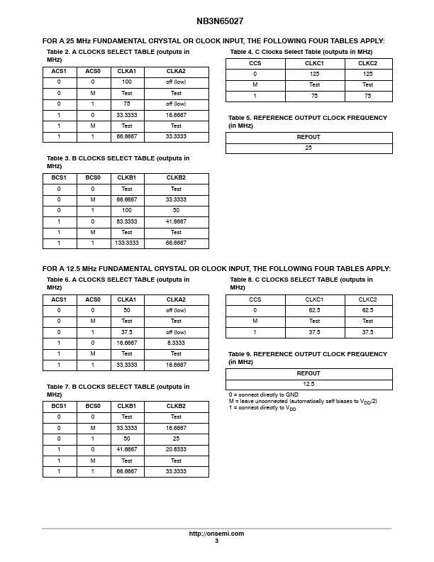
- 12.5 MHz or 25 MHz Fundamental Crystal or Clock
- Six Output Clocks with Selectable Frequencies
- Buffered Crystal Reference Output
- SDRAM Frequencies of 67, 83, 100, and 133 MHz
- Operating Range: VCC = 3.3 V ±10%
- QSOP-20 Package, 150 mil
- 40°C to +85°C Ambient Operating Temperature
- These Devices are Pb-Free and are RoHS pliant
- LVCMOS with 25 mA Output Drive Capability at TTL
- Rev. 2