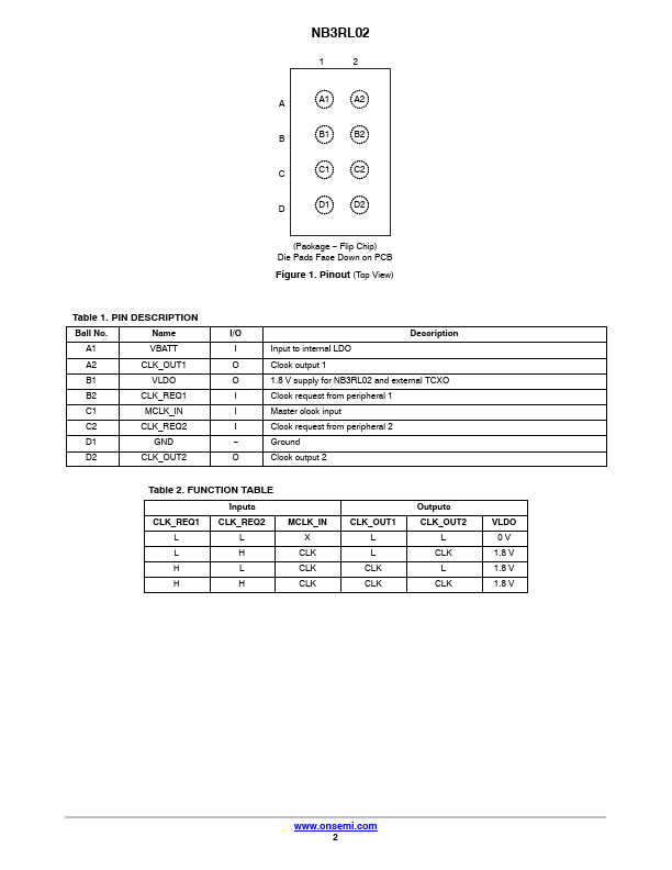
Datasheet4U Logo Datasheet4U.com

NB3RL02 - Low Phase-Noise Two-Channel Clock Fanout Buffer

General Description

Ball No.

Key Features

  • Low Additive Noise:.
  • 149 dBc/Hz at 10 kHz Offset Phase Noise.
  • 0.37 ps (rms) Output Jitter.
  • Limited Output Slew Rate for EMI Reduction (1 ns to 5 ns/Rise/Fall Time for 10.
  • 50 pF Loads).
  • Regulated 1.8 V Output Supply Available for External Clock Source, ie. TCX0.
  • Operation to 80 MHz.
  • Ultra.
  • Small Package:.
  • 8.
  • ball: 0.4 mm Pitch WLCS.
  • ESD Performance Exceeds JESD 22.
  • 2000 V Human.

📥 Download Datasheet

Datasheet Details

Part number NB3RL02
Manufacturer onsemi
File Size 277.47 KB
Description Low Phase-Noise Two-Channel Clock Fanout Buffer
Datasheet download datasheet NB3RL02 Datasheet

Full PDF Text Transcription (Reference)

The following content is an automatically extracted verbatim text from the original manufacturer datasheet and is provided for reference purposes only.

View original datasheet text
NB3RL02 Low Phase-Noise Two-Channel Clock Fanout Buffer The NB3RL02 is a low−skew, low jitter 1:2 clock fan−out buffer, ideal for use in portable end−equipment, such as mobile phones. With integrated LDO and output control circuitry. The MCLK_IN pin has an AC coupling capacitor and will directly accept a square or sine wave clock input, such as a temperature compensated crystal oscillator (TCXO). The minimum acceptable input amplitude of the sine wave is 300 mV peak−to−peak. The two clock outputs are enabled by control inputs CLK_REQ1 and CLK_REQ2. The NB3RL02 has an integrated Low−Drop−Out (LDO) voltage regulator which accepts input voltages from 2.3 V to 5.5 V and outputs 1.8 V at Iout = 50 mA. This 1.