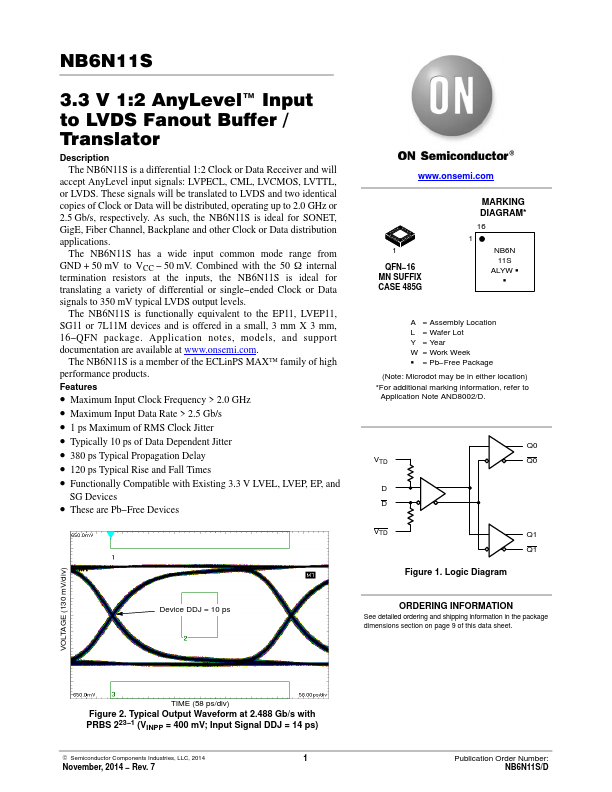
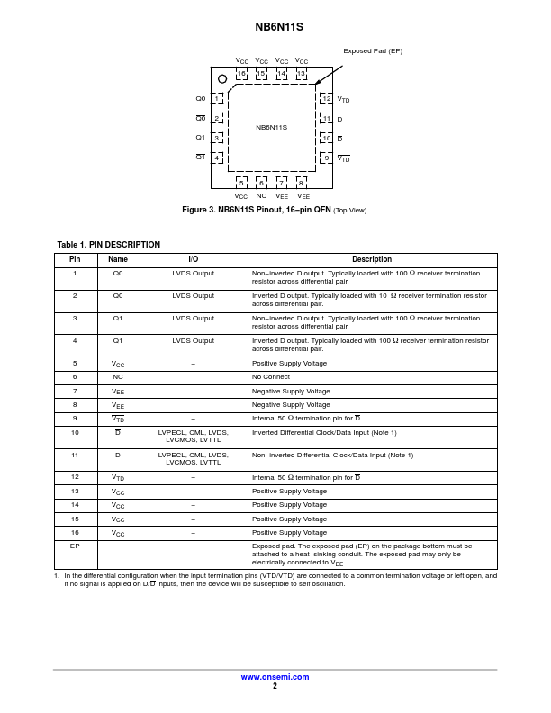
NB6N11S Overview
The NB6N11S is a differential 1:2 Clock or Data Receiver and will accept AnyLevel input signals: LVPECL, CML, LVCMOS, LVTTL, or LVDS. These signals will be translated to LVDS and two identical copies of Clock or Data will be distributed, operating up to 2.0 GHz or 2.5 Gb/s, respectively.
NB6N11S Key Features
- Maximum Input Clock Frequency > 2.0 GHz
- Maximum Input Data Rate > 2.5 Gb/s
- 1 ps Maximum of RMS Clock Jitter
- Typically 10 ps of Data Dependent Jitter
- 380 ps Typical Propagation Delay
- 120 ps Typical Rise and Fall Times
- Functionally patible with Existing 3.3 V LVEL, LVEP, EP, and
- These are Pb-Free Devices
- For additional marking information, refer to Application Note AND8002/D
- Rev. 7