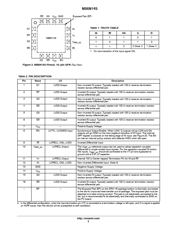
Datasheet4U Logo Datasheet4U.com

NB6N14S Datasheet Differential Input to LVDS Fanout Buffer/Translator

Manufacturer: onsemi

Datasheet Details

Part number NB6N14S
Manufacturer onsemi
File Size 367.51 KB
Description Differential Input to LVDS Fanout Buffer/Translator
Datasheet download datasheet NB6N14S Datasheet

Overview

NB6N14S 3.3 V 1:4 AnyLevelt Differential Input to LVDS Fanout Buffer/Translator The NB6N14S is a differential 1:4 Clock or Data Receiver and will accept AnyLevelt differential input signals: LVPECL, CML or LVDS.

These signals will be translated to LVDS and four identical copies of Clock or Data will be distributed, operating up to 2.0 GHz or 2.5 Gb/s, respectively.

As such, the NB6N14S is ideal for SONET, GigE, Fiber Channel, Backplane and other Clock or Data distribution applications.

Key Features

  • Maximum Input Clock Frequency > 2.0 GHz.
  • Maximum Input Data Rate > 2.5 Gb/s.
  • 1 ps Maximum RMS Clock Jitter.
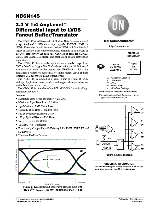
  • Typically 10 ps Data Dependent Jitter.
  • 380 ps Typical Propagation Delay.
  • 120 ps Typical Rise and Fall Times.
  • VREF_AC Reference Output.
  • TIA/EIA.
  • 644 Compliant.
  • Functionally Compatible with Existing 3.3 V LVEL, LVEP, EP, and SG Devices.
  • These are Pb.
  • Free Devices Device DDJ = 10 ps htt.