Datasheet4U Logo Datasheet4U.com

NBSG111 Datasheet - ON Semiconductor

2.5V/3.3V SiGe Differential 1:10 Clock/Data Driver

NBSG111 Features

* Maximum Input Clock Frequency > 6 GHz Typical

* Maximum Input Data Rate > 6 Gb/s Typical

* 300 ps Typical Propagation Delay

* 60 ps Typical Rise and Fall Times

* RSPECL Output with Operating Range: VCC = 2.375 V to 3.465 V with VEE = 0 V

* RSNECL Out

NBSG111 General Description

The NBSG111 is a 1 *to *10 differential clock/data driver. The device is functionally equivalent to the LVEP111 device with much higher bandwidth and lower EMI capabilities. 
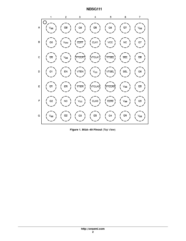
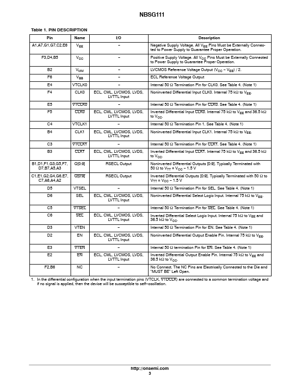
Inputs incorporate internal 50 W termination resistors (input to VT pad) and accept NECL (Negative ECL), PECL (P.

NBSG111 Datasheet (143.81 KB)

Preview of NBSG111 PDF

Datasheet Details

Part number:

NBSG111

Manufacturer:

ON Semiconductor ↗

File Size:

143.81 KB

Description:

2.5v/3.3v sige differential 1:10 clock/data driver.

📁 Related Datasheet

NBSG11 2.5V/3.3VSiGe 1:2 Differential Clock Driver with RSECL* Outputs (ON)

NBSG11BA 2.5V/3.3VSiGe 1:2 Differential Clock Driver with RSECL* Outputs (ON)

NBSG11BAEVB 2.5V/3.3VSiGe 1:2 Differential Clock Driver with RSECL* Outputs (ON)

NBSG11BAR2 2.5V/3.3VSiGe 1:2 Differential Clock Driver with RSECL* Outputs (ON)

NBSG11MN 2.5V/3.3VSiGe 1:2 Differential Clock Driver with RSECL* Outputs (ON)

NBSG11MNR2 2.5V/3.3VSiGe 1:2 Differential Clock Driver with RSECL* Outputs (ON)

NBSG14 SiGe Differential 1:4 Clock/Data Driver (ON Semiconductor)

NBSG16 SiGe Differential Receiver/Driver (ON Semiconductor)

NBSG16M 2.5V/3.3VMultilevel Input to CML Clock/Data Receiver/Driver/Translator Buffer (ON)

NBSG16MMN 2.5V/3.3VMultilevel Input to CML Clock/Data Receiver/Driver/Translator Buffer (ON)

TAGS

NBSG111 2.5V 3.3V SiGe Differential 110 Clock Data Driver ON Semiconductor

Image Gallery

NBSG111 Datasheet Preview Page 2 NBSG111 Datasheet Preview Page 3

NBSG111 Distributor