logo

NBXSBA019 Datasheet, ON Semiconductor

NBXSBA019 Datasheet, ON Semiconductor

NBXSBA019

datasheet Download (Size : 156.74KB)

NBXSBA019 Datasheet

NBXSBA019 oscillator equivalent, clock oscillator.

NBXSBA019

datasheet Download (Size : 156.74KB)

NBXSBA019 Datasheet

Features and benefits

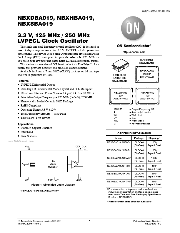
http://onsemi.com MARKING DIAGRAMS NBXDBA019 125/250 AWLYYWWG 6 PIN CLCC LN SUFFIX CASE 848AB
*
*
*
*
*
*
*
*
* LVPECL Differential.

Application

The device uses a high Q fundamental crystal and Phase Lock Loop (PLL) multiplier to provide selectable 125 MHz or 250 .

Description

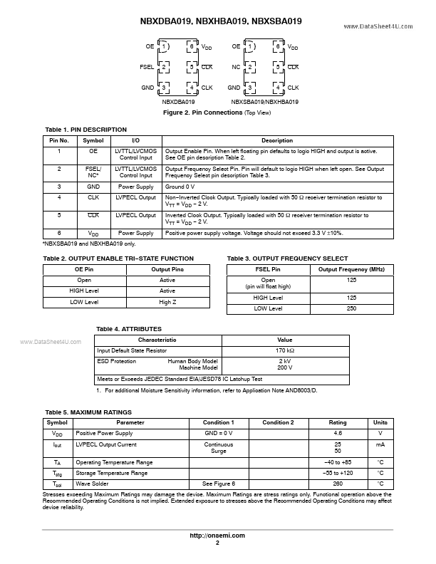
LVTTL/LVCMOS Control Input LVTTL/LVCMOS Control Input Power Supply Output Enable Pin. When left floating pin defaults to logic HIGH and output is active. See OE pin description Table 2. FSEL/ NC* GND CLK CLK VDD Output Frequency Select Pin. Pin will .

Image gallery

NBXSBA019 Page 1 NBXSBA019 Page 2 NBXSBA019 Page 3

TAGS

NBXSBA019
Clock
Oscillator
ON Semiconductor

Manufacturer


ON Semiconductor (https://www.onsemi.com/)

Related datasheet

NBXSBA010

NBXSBA017

NBXSBA007

NBXSBA008

NBXSBA020

NBXSBA021

NBXSBA022

NBXSBA023

NBXSBA024

NBXSBA025

NBXSBA051

NBXSBB020

NBXSBB021

Since 2006. D4U Semicon.   |   Contact Us   |   Privacy Policy   |   Purchase of parts