NCP139
features low IQ consumption. The WLCSP6 1.2 mm x 0.8 mm Chip Scale package is optimized for use in space constrained applications.
Features
- Input Voltage Range: VOUT to 5.5 V
- Bias Voltage Range: 3.0 V to 5.5 V
- Adjustable and Fixed Voltage Version Available
- Output Voltage Range: 0.4 V to 1.8 V (Fixed)
Output Voltage Range 0.5 V to 3.0 V (Adjustable)
- ±1% Accuracy over Temperature, 0.5% VOUT @ 25°C
- Ultra- Low Dropout: Typ. 50 m V at 1 A
- Very Low Bias Input Current of Typ. 35 m A
- Very Low Bias Input Current in Disable Mode: Typ. 0.5 m A
- Logic Level Enable Input for ON/OFF Control
- Output Active Discharge Option Available
- Stable with a 10 m F Ceramic Capacitor
- Available in WLCSP6
- 1.2 mm x 0.8 mm, 0.4 mm pitch Package
- These Devices are Pb- Free, Halogen Free/BFR Free and are Ro HS pliant
Typical Applications
- Battery- powered Equipment
- Smartphones, Tablets
- Cameras, DVRs, STB and Camcorders
DATA SHEET .onsemi.
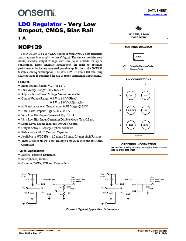
WLCSP6, 1.2x0.8 CASE 567MV T
MARKING DIAGRAM
XX =...