NCP189
NCP189 is LDO Regulator manufactured by onsemi.
Features
- Operating Input Voltage Range: 1.6 V to 5.5 V
- Available in Fixed Voltage Option: 0.6 V to 5.0 V
- Adjustable Version Reference Voltage: 0.6 V
- ±0.7% Initial Accuracy at 25°C
- ±1% Accuracy Over Load and Temperature
- Low Quiescent Current Typ. 35 m A
- Shutdown Current: Typ. 0.1 m A
- Very Low Dropout: Typ. 65 m V at 500 m A for 3.3 V Variant
- High PSRR: Typ. 85 d B at 100 m A, f = 1 k Hz
- Low Noise: 10 m VRMS (Fixed Version)
- Stable with a 4.7 m F Small Case Size Ceramic Capacitors
- Controlled Output Voltage Slew Rate from 5 m V / ms
- Available in WDFNW6 2 mm x 2 mm x 0.75 mm Case 511DW
- These Devices are Pb- Free, Halogen Free/BFR Free and are Ro HS pliant
Typical Applications
- munication Systems
- In- Vehicle Networking
- Telematics, Infotainment and Clusters
- General Purpose Automotive
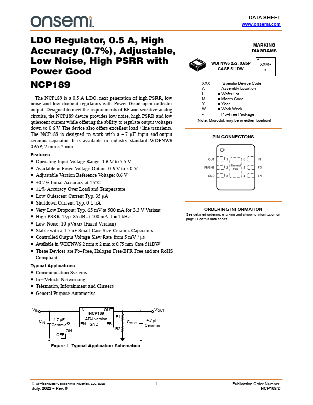
MARKING DIAGRAMS
WDFNW6 2x2, 0.65P CASE 511DW
XXMG G
XXX A L M Y W G
= Specific Device Code = Assembly Location = Wafer Lot = Month Code = Year = Work Week = Pb- Free Package
(Note: Microdot may be in either location)
PIN CONNECTONS
ORDERING INFORMATION
See detailed ordering, marking and shipping information on page 11 of this data sheet.
4.7 m F Ceramic
ON OFF
ADJ version R1
EN GND FB
R2
COUT
VOUT
4.7 m F Ceramic
Figure 1. Typical Application...