Description
Input pin Ground pin Chip enable pin (“H” active) Non connected Output pin Exposed Pad (leave floating or connect to GND) Rating Symbol Value Unit Input Voltage (Note 1) Output Voltage VIN VOUT -0.3 to 12 -0.3 to VIN ≤ 11 V V Chip Enable Input VCE -0.3 to VIN ≤ 11 V Power Dissipation SOT-23-5 Power Dissipation uDFN 1.0 x 1.0 mm PD 420 mW 400 Power Dissipation SC-88A 380 Junction Temperature TJ -40 to 150 °C Storage Temperature TSTG -55 to 125 °C ESD Capability, Human Body Model (Note 2) ESDHBM 2000 V ESD Capability, Machine Model (Note 2) ESDMM 200 V Stresses exceeding those listed in the ESD Human Body Model tested per AEC-Q100-002 (EIA/JESD22-A114) ESD Machine Model tested per AEC-Q100-003 (EIA/JESD22-A115) Latchup Current Maximum Rating tested per JEDEC standard: JESD78.
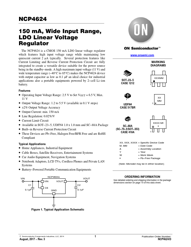
Key Features
- Operating Input Voltage Range: 2.5 V to Set VOUT + 6.5 V, Max. 11 V
- Output Voltage Range: 1.2 to 5.5 V (available in 0.1 V steps)
- ±2% Output Voltage Accuracy
- Output Current: min. 150 mA
- Line Regulation: 0.02%/V
- Current Limit Circuit
- Built-in Reverse Current Protection Circuit
- These Devices are Pb-Free, Halogen Free/BFR Free and are RoHS pliant
Applications
- Cable Boxes, Satellite Receivers, Entertainment Systems