NCP51145 Description
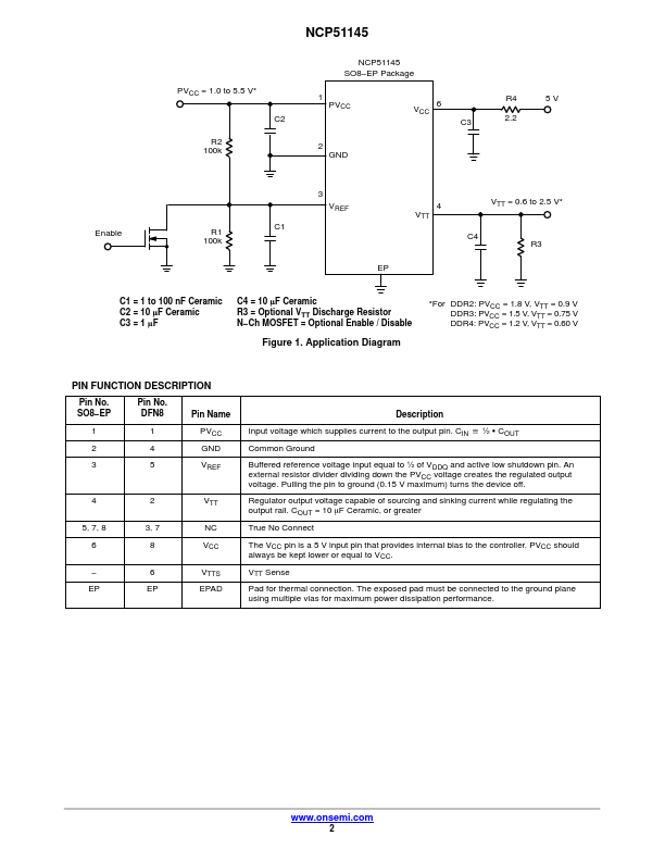
Pin No. SO8−EP Pin No. DFN8 Pin Name 1 1 PVCC 2 4 GND 3 5 VREF 4 2 VTT 5, 7, 8 6 3, 7 8 NC VCC − 6 VTTS EP EP EPAD Description Input voltage which supplies current to the output pin. CIN ^.
NCP51145 Key Features
- For DDR VTT
NCP51145 Applications
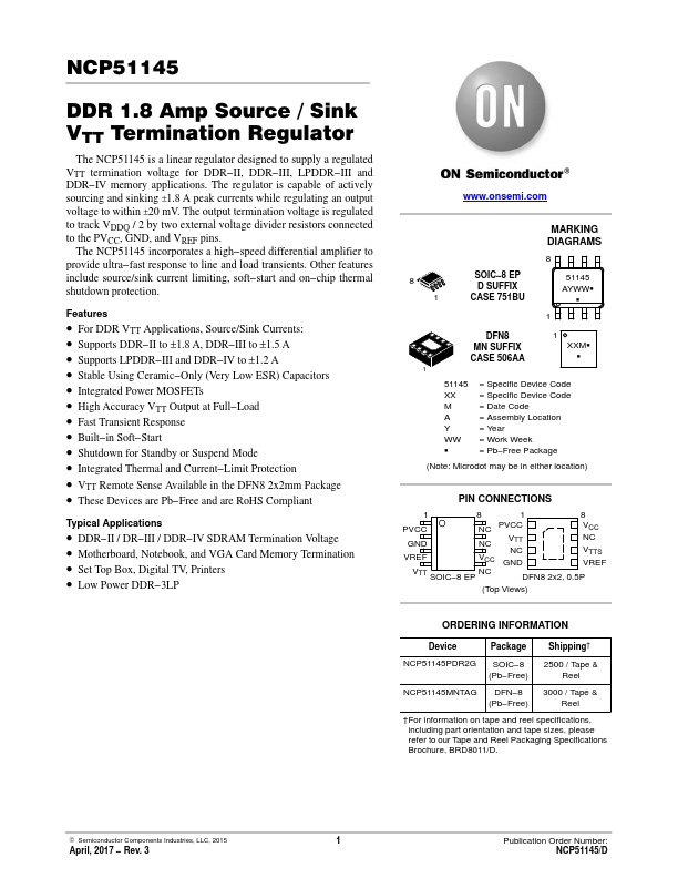
- For DDR VTT Applications, Source/Sink Currents
- Supports DDR−II to ±1.8 A, DDR−III to ±1.5 A
- Supports LPDDR−III and DDR−IV to ±1.2 A


