Datasheet4U Logo Datasheet4U.com
7 views

NCP51199 Datasheet - ON Semiconductor

NCP51199 Termination Regulator

Pin No. 
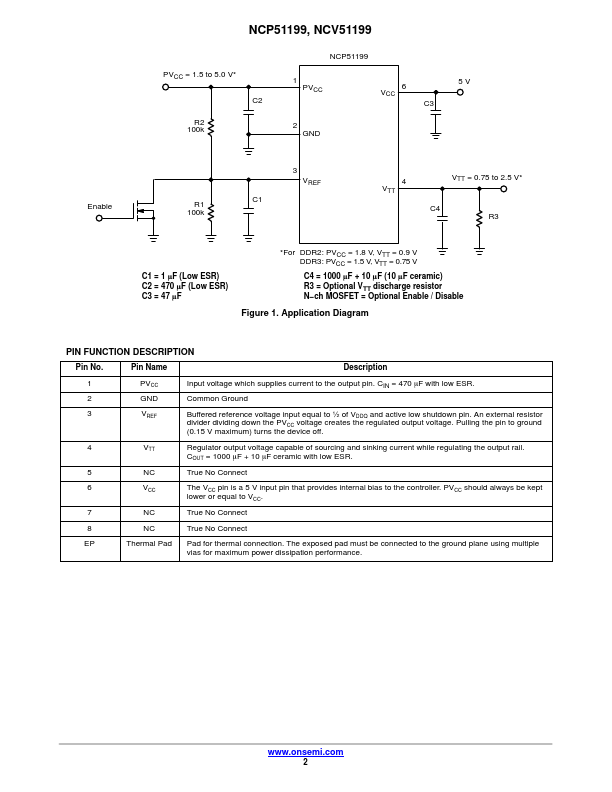
Pin Name Description 1 PVCC Input voltage which supplies current to the output pin. CIN = 470 mF with low ESR. 2 GND Common Ground 3 VREF Buffered reference voltage input equal to ½ of VDDQ and active low shutdown pin. An external resistor divider dividing down the PVCC voltage .
NCP51199, NCV51199 DDR 2-Amp Source / Sink VTT Termination Regulator The NCP/NCV51199 is a linear regulator designed to supply a regulated VTT termination voltage for DDR 2 and DDR 3 memory applications. The regulator is capable of actively sourcing and sinking ±2 A peak currents for DDR 2, and DDR 3 up to ±1.5 A while regulating the VTT output voltage to within ±10 mV. The output termination voltage is regulated to track VDDQ / 2 by two external voltage divider .

NCP51199 Features

* include source/sink current limiting, soft

* start and on

* chip thermal shutdown protection. Features

* Supports DDR

* 2 VTT Termination to ±2 A, DDR

* 3 to ±1.5 A (peak)

* Stable with 10 mF Ceramic Capacitance on VTT Output

* Integrated Power MOSFETs

NCP51199-ONSemiconductor.pdf

Preview of NCP51199 PDF
NCP51199 Datasheet Preview Page 2 NCP51199 Datasheet Preview Page 3

Datasheet Details

Part number:

NCP51199

Manufacturer:

ON Semiconductor ↗

File Size:

67.39 KB

Description:

Termination regulator.

NCP51199 Distributor

📁 Related Datasheet

📌 TAGS

Stock and price

Distributor
FIBOX
UL CAB PC 302018 T
3 In Stock
Qty : 1 units
Unit Price : $184.39