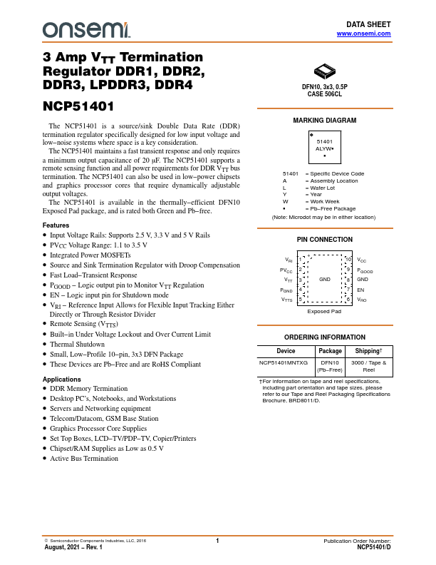
NCP51401 Description
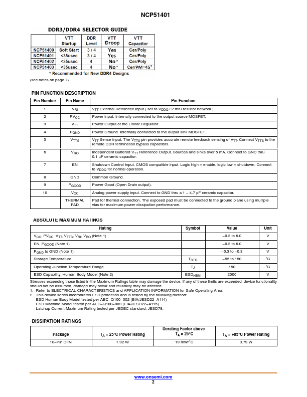
Pin Number Pin Name Pin Function 1 VRI VTT External Reference Input ( set to VDDQ / 2 thru resistor network ). Internally connected to the output source MOSFET. 3 VTT Power Output of the Linear Regulator.
NCP51401 Key Features
- Input Voltage Rails: Supports 2.5 V, 3.3 V and 5 V Rails
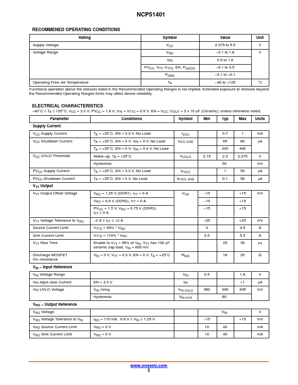
- PVCC Voltage Range: 1.1 to 3.5 V
- Integrated Power MOSFETs
- Source and Sink Termination Regulator with Droop pensation
- Fast Load-Transient Response
- Logic output pin to Monitor VTT Regulation
- Logic input pin for Shutdown mode
- Reference Input Allows for Flexible Input Tracking Either
- Remote Sensing (VTTS)
- Built-in Under Voltage Lockout and Over Current Limit